One of the first arcades I'm buying that caught my attention was the NSS, Nintendo Super System. I'm going to be going over a lot of information this post so feel free to freely skim through it.
First of all.. the arcade cabinet in question is a Nintendo Super System or 'NSS' for short. The NSS is an arcade system used to preview Super NES games in the United States. It is essentially the Super NES hardware with a menu interface that—similar to Nintendo's PlayChoice-10 hardware for NES games—allows players to play select Super NES games for a certain amount of time, depending on how many game credits they insert.
Game cartridges available for this cabinet include (but limited to 3 at once)...
- ActRaiser
- The Addams Family
- Contra III: The Alien Wars
- David Crane's Amazing Tennis
- F-Zero
- Lethal Weapon
- NCAA Basketball
- Robocop 3
- The Irem Skins Game
- Super Mario World
- Super Soccer
- Super Tennis
+++++++++++++++++++++++++


+++++++++++++++++++++++++
So you're probably thinking... "does it play regular Super Nintendo games?" Well, no and yes.
Awhile back a fan-made creation known as the "SNES/SFC to Nintendo Super System Adapter" showed up. He ended up producing a few models of it but has since then stopped developing the adapter. I've been looking for a used copy but they are quite rare and I'd imagine those who do own one, don't want to easily give it up.
So I've gone on a quest to learn as much about them as I can to possibly have my own or get someone else to develop a few again (I need at least 5 myself).
Here's photos of the .pdf file that came with the original adapter...


+++++++++++++++++++++++++
I found all these details at http://problemkaputt.de/fullsnes.htm under 'SNES Hotel Boxes and Arcade Machines.'
Nintendo Super System (NSS) (USA) (1991)
Arcade Cabinet. Contains up to three special cartridges (with one game each).
001- NSS Memory and I/O Maps
002- NSS I/O Ports - Control Registers
003- NSS I/O Ports - Button Inputs and Coin Control
004- NSS I/O Ports - RTC and OSD
005- NSS I/O Ports - EEPROM and PROM
006- NSS BIOS and INST ROM Maps
007- NSS Interpreter Tokens
008- NSS Controls
009- NSS Games, BIOSes and ROM-Images
010- NSS Component Lists
011- NSS On-Screen Controller (OSD)
012- SNES Pinouts NSS Connectors
013- Z80 CPU Specifications
001- NSS Memory and I/O MapsZ80 Memory Map
  0000h-7FFFh : 32K BIOS
  8000h-9FFFh : 8K RAM (upper 4K with write-protect)
  A000h       : EEPROM Input (R)
  C000h-DFFFh : Upper 8K of 32K Instruction EPROM (in Cartridge) (INST-ROM)
  E000h       : EEPROM Output (W)
  Exxxh       : PROM Input AND Output AND Program Code (RST opcodes) (R/W/EXEC)
|
Z80 IN-Ports
  Port 00h.R - IC46/74LS540 - Joypad Buttons and Vsync Flag
  Port 01h.R - IC38/74LS540 - Front-Panel Buttons & Game Over Flag
  Port 02h.R - IC32/74LS540 - Coin and Service Buttons Inputs
  Port 03h.R - IC31/74HC367 - Real-Time Clock (RTC) Input
  Port 04h.R - Returns FFh (unused)
  Port 05h.R - Returns FFh (unused)
  Port 06h.R - Returns FFh (unused)
  Port 07h.R - Returns FFh (same effect as write-any-value to Port 07h.W)
|
Z80 OUT-Ports
  Port 00h/80h.W         - IC40/74HC161 - NMI Control and RAM-Protect
  Port 01h/81h.W         - IC39/74HC377 - Unknown and Slot Select
  Port 02h/82h/72h/EAh.W - IC45/74HC377 - RTC and OSD
  Port 03h/83h.W         - IC47/74HC377 - Unknown and LED control
  Port 84h.W             - IC25/74HC161 - Coin Counter Outputs
  Port 05h.W             - Unused (bug: written by mistake)
  Port 06h.W             - Unused
  Port 07h.W - IC23/74HC109 - SNES Watchdog: Acknowledge SNES Joypad Read Flag
|
SNES Memory Map
Normal SNES memory map, plus some special registers:
  4100h/Read.Bit0-7  - DIP-Switches (contained in some NSS cartridges)
  4016h/Write.Bit0   - Joypad Strobe (probably clears the SNES Watchdog flag?)
                          (OR, maybe that occurs not on 4016h-writes,
                          but rather on 4016h/4017h-reads, OR elsewhere?)
  4016h/Write.Bit2   - Joypad OUT2 indicates Game Over (in Skill Mode games)
  4016h/4017h/4218h..421Bh - Joypad Inputs (can be disabled)


002- NSS I/O Ports - Control Registers
Port WHERE.WSomewhere, following OUTPUT signals should be found:
  SNES Reset Signal (maybe separate CPU/PPU resets, and stop, as on PC10)
  SNES Joypad Disable
  SNES Power Supply Enable (SNES VCC switched via Q1 transistor)
  Maybe support for sending data from Z80 to SNES (eg. to 4016h/4017h/4213h)?
|
Port 00h/80h.W - NMI Control and RAM-Protect (IC40/74HC161)
  7-4 Unknown/unused      (should be always 0)
  3     Maybe SNES CPU/PPU reset (usually same as Port 01h.W.Bit1)
  2   RAM at 9000h-9FFFh  (0=Disable/Protect, 1=Enable/Unlock)
  1     Looks like maybe somehow NMI Related ?  ;\or one of these is PC10-style
  0     Looks like NMI Enable                   ;/hardware-watchdog reload?
|
Port 01h/81h.W - Unknown and Slot Select (IC39/74HC377)
  7     Maybe SNES Joypad Enable? (0=Disable/Demo, 1=Enable/Game)
  6   Unknown/unused        (should be always 0)
  5   SNES Sound Mute       (0=Normal, 1=Mute) (for optional mute in demo mode)
  4   Player 2 Controls (0=CN4 Connector, 1=Normal/Joypad 2) (INST ROM Flags.0)
  3-2 Slot Select (0..2=1st..3rd Slot, 3=None) (mapping to both SNES and Z80)
  1     Maybe SNES CPU pause?  (cleared on deposit coin to continue) (1=Run)
  0     Maybe SNES CPU/PPU reset?   (0=Reset, 1=Run)
|
Port 03h/83h.W - Unknown and LED control (IC47/74HC377)
  7     Layer SNES Enable?             (used by token proc, see 7A46h) SNES?
  6     Layer OSD Enable?
  5-4 Unknown/unused (should be always 0)
  3   LED Instructions (0=Off, 1=On)  ;-glows in demo (prompt for INST button)
  2   LED Game 3       (0=Off, 1=On)  ;\
  1   LED Game 2       (0=Off, 1=On)  ; blinked when enough credits inserted
  0   LED Game 1       (0=Off, 1=On)  ;/
|
Port 05h.W - Unused/Bug
7-0 Unknown
|
Port 07h.W - SNES Watchdog: Acknowledge SNES Joypad Read Flag (IC23/74HC109)
7-0 Unknown/unused (write any dummy value)
|
If the watchdog expires more than once, then the game is removed from the cartridge list, and used credits are returned to the user (then allowing to play other games; as long as there are any other games installed).
Note: Judging from hardware tests, there seem to be other ways to acknowledge the flag (probably via Port 07h.R, or maybe even via Port 00h.R itself).
NMI
The NMI source is unknown. Maybe Vblank/Vsync, maybe from SNES or OSD, or some other timer signal.
Game/Demo-Mode Detection
The original NSS games seem to be unable to detect if a coin is inserted (ie. if they should enter game or demo mode). However, it's possible to do that kind of detection:
Joypad Disable does work much like disconnecting the joypad, so one can check the 17th joypad bit to check if the joypad is connected/enabled (aka if money is inserted). The Magic Floor game is using that trick to switch between game and demo mode (this has been tested by DogP and works on real hardware, ie. the NSS does really disable the whole joypad bitstream, unlike the PC10 which seems to disable only certain buttons).
003- NSS I/O Ports - Button Inputs and Coin Control Port 00h.R - Joypad Buttons (IC46/74LS540)
  7   SNES Watchdog (0=SNES did read Joypads, 1=Didn't do so) (ack via 07h.W)
  6   Vsync (from OSD or SNES ?)  (0=Vsync, 1=No) (zero for ca. 3 scanlines)
  5   Button "Joypad Button B?"   (0=Released, 1=Pressed)
  4   Button "Joypad Button A"    (0=Released, 1=Pressed)
  3   Button "Joypad Down"        (0=Released, 1=Pressed)
  2   Button "Joypad Up"          (0=Released, 1=Pressed)
  1   Button "Joypad Left"        (0=Released, 1=Pressed)
  0   Button "Joypad Right"       (0=Released, 1=Pressed)
|
Port 01h.R - Front-Panel Buttons & Game Over Flag (IC38/74LS540)
  7   From SNES Port 4016h.W.Bit2 (0=Game Over Flag, 1=Normal) (Inverted!)
  6   Button "Restart"            (0=Released, 1=Pressed) ;-also resets SNES?
  5   Button "Page Up"            (0=Released, 1=Pressed)
  4   Button "Page Down"          (0=Released, 1=Pressed)
  3   Button "Instructions"       (0=Released, 1=Pressed)
  2   Button "Game 3"             (0=Released, 1=Pressed) ;\if present (single
  1   Button "Game 2"             (0=Released, 1=Pressed) ; cartridge mode does
  0   Button "Game 1"             (0=Released, 1=Pressed) ;/work without them)
|
Port 02h.R - Coin and Service Buttons Inputs (IC32/74LS540)
  7-3 External 5bit input (usually CN5 isn't connected: always 0=High)
  2   Service Button (1=Pressed: Add Credit; with INST button: Config)
  1   Coin Input 2   (1=Coin inserted in coin-slot 2)
  0   Coin Input 1   (1=Coin inserted in coin-slot 1)
|
Port 84h.W - Coin Counter Outputs (IC25/74HC161)
  7-4 Unknown/unused (should be always 0) (probably not connected anywhere)
  3-2 Unknown/unused (should be always 0) (probably wired to 74HC161)
  1   Coin Counter 2 (0=No change, 1=Increment external counter)
  0   Coin Counter 1 (0=No change, 1=Increment external counter)
|
004- NSS I/O Ports - RTC and OSD Real-Time Clock (RTC) and On-Screen Display (OSD) Registers
Port 03h.R - Real-Time Clock (RTC) Input (IC31/74HC367)
  7-1 Unknown/unused    (seems to be always 7Eh, ie. all seven bits set)
  0   RTC Data In       (0=Low=Zero, 1=High=One)
|
Port 02h/82h/72h/EAh.W - RTC and OSD (IC45/74HC377)
  7   OSD Clock ?       (usually same as Bit6)  ;\Chip Select when Bit6=Bit7 ?
  6   OSD Clock ?       (usually same as Bit7)  ;/
  5   OSD Data Out      (0=Low=Zero, 1=High=One)
  4   OSD Special       (?)  ... or just /CS ? (or software index DC3F/DD3F?)
  3   RTC /CLK          (0=Low=Clock,  1=High=Idle)              ;S-3520
  2   RTC Data Out      (0=Low=Zero,   1=High=One)
  1   RTC Direction     (0=Low=Write,  1=High=Read)
  0   RTC /CS           (0=Low/Select, 1=High/No)
|
RTC Real-Time Clock (S-3520)
The NSS-BIOS supports year 1900..2099 (century 00h=19xx, FFh=20xx is stored in RAM at 8F8Dh/978Dh/9F8Dh; in the two version "03" BIOSes). The current time is shown when pressing Restart in the Bookkeeping screen.
Seiko/Epson S-3520CF Serial 4bit Real-Time Clock (RTC)
Contains the usual Time/Date registers, plus 120bit battery-backed RAM (aka 15 bytes) (organized in 2 pages of 15 x 4bits).
This chip is used in both Nintendo Super System (NSS), and in Super Famicom Box.
Seiko/Epson S-3520CF Register Table
  Index  Bit3   Bit2   Bit1    Bit0  ;Expl.
  ___Registers in Mode 0_____________ ______________
  0      Sec3   Sec2   Sec1    Sec0  ;Seconds, Low     ;\
  1      0      Sec6   Sec5    Sec4  ;Seconds, High    ;
  2      Min3   Min2   Min1    Min0  ;Minutes, Low     ; Read/Increment-able
  3      0      Min6   Min5    Min4  ;Minutes, High    ;
  4      Hour3  Hour2  Hour1   Hour0 ;Hours, Low       ; (reading returns the
  5      PM/AM  0      Hour5   Hour4 ;Hours, High      ; counter value)
  6      0      Week2  Week1   Week0 ;Day of Week      ;
  7      Day3   Day2   Day0    Day0  ;Day, Low         ; (writing any dummy
  8      0      0      Day5    Day4  ;Day, High        ; value does increment
  9      Mon3   Mon2   Mon1    Mon0  ;Month, Low       ; counter value by 1)
  A      0      0      0       Mon4  ;Month, High      ;
  B      Year3  Year2  Year1   Year0 ;Year, Low        ;
  C      Year7  Year6  Year5   Year4 ;Year, High       ;/
  D      TPS    30ADJ  CNTR    24/12 ;Control Register ;-Read/Write-able
  E      STA    LOST   0       0     ;Status Register  ;-Read only
  ___Registers in Mode 1_____________ ________________
  0-E    x      x      x       x     ;Reserved         ;-Don't use
  ___Registers in Mode 2_____________ ________________
  0-E    SRAM   SRAM   SRAM    SRAM  ;SRAM Page 0      ;-Read/Write-able
  ___Registers in Mode 3_____________ ________________
  0-E    SRAM   SRAM   SRAM    SRAM  ;SRAM Page 1      ;-Read/Write-able
  ___Mode Register (in Mode 0..3)____ ________________
  F      SYSR   TEST   Mode1   Mode0 ;Mode Register    ;-Read/Write-able
|
  Sec    Seconds (BCD, 00h..59h)
  Min    Minutes (BCD, 00h..59h)
  Hour   Hours   (BCD, 00h..23h or 01h..12h)
  Day    Day     (BCD, 01h..31h)
  Month  Month   (BCD, 01h..12h)
  Year   Year    (BCD, 00h..99h)
  Week   Day of Week (0..6) (SFC-Box: Unknown assignment) (NSS: 0=Sunday)
  PM/AM  Set for PM, cleared for AM (this is done even when in 24-hour mode)
  24/12  24-Hour Mode (0=12, 1=24) (Time/Date may get corrupted when changed?)
  TPS    Select Reference Waveform for output on Pin8 (0=1024Hz, 1=1Hz)
  30ADJ  Set seconds to zero, and, if seconds was>=30, increase minutes
  CNTR   Reset Counters (0=Normal, 1=Reset)
  SYSR   Reset Counters and Control/Status/Mode Registers (0=Normal, 1=Reset)
  LOST   Time Lost (0=Okay, 1=Lost/Battery failure) (can be reset... how?)
  STA    Time Stable (0=Stable/Sec won't change in next 3.9ms, 1=Unstable)
  Mode   Mode for Register 0-E (0=RTC, 1=Reserved, 2=SramPage0, 3=SramPage1)
|
Serial Access
Set /CLK and /CS to HIGH as default level. Set /WR to desired direction (before dragging /CS low). Then set /CS to LOW to invoke transfer. Then transfer index/data/garbage (usually 8 clks for WRITES, and 16 clks for READS). Then set /CS back HIGH.
Index/Data/Garbage Nibbles are 4bit each (transferred LSB first). Bits should be output (to DataIn) on falling CLK edge (note: the NSS is doing that properly, the SFC-Box actually outputs data shortly after falling CLK), and can be read (from DataOut) at-or-after raising CLK edge. The separate nibbles are:
  Nibble   To RTC                       From RTC
  1st      Index I                      Garbage (old index or so)
  2nd      Data I    (or dummy)         Garbage (data from old index or so)
  3rd      Index II  (or dummy)         Garbage (index I or so)
  4th      Data II   (or dummy)         Data I
  5th      Index III (or dummy)         Garbage (index II or so)
  6th      Data III  (or dummy)         Data II
|
For Reads, one needs to send/receive at least 4 nibbles (though most of them are dummies/garbage; actually used are 1st-To-RTC, and 4th-From-RTC). If desired, one can read two or more registers by reading/writing 6 or more nibbles (the NSS BIOS does so).
Pin-Outs
SNES Pinouts RTC Chips
Sharp S-RTC Pin-Outs (used by Dai Kaiju Monogatari 2)
1-24 Unknown (should have an address decoder and 4bit data bus or so)
|
Epson/Seiko RTC-4513 Pin-Outs (for Far East of Eden Zero) (via SPC7110 chip)
  1 NC
  2 DATA
  3 STD.P
  4 NC
  5 NC
  6 VCC
  7 NC
  8 NC
  9 GND
  10 NC
  11 NC
  12 CE
  13 CLK
  14 NC
|
Seiko/Epson S-3520CF Pin-Outs (used in SFC-Box and NSS)
  1 Xin
  2 NC
  3 Xout
  4 /CLK
  5 DataIn
  6 /WR
  7 GND
  8 /TPOUT
  9 DataOut
  10 PDW
  11 /CS
  12 Capacitor
  13 NC
  14 VCC
|
OSD On-Screen Display (M50458-001SP)On-Screen Display Controller M50458-001SP (Mitsubishi Microcomputers)
OSD Addresses
The OSD Address is transferred as first word (after chip select):
  0000h..011Fh  Character RAM (24x12 tiles, aka 288 tiles, aka 120h tiles)
  0120h..0127h  Configuration Registers (8 registers)
|
Character Codes (for OSD Address 000h..011Fh)
  0-6   Character Number (non-ASCII)
  7     Unused (zero)
  8-10  Text Color     (on NSS: 3bit RGB) (Bit0=Red, Bit1=Green, Bit2=Blue)
  11    Blinking flag  (0=Normal, 1=Blink)
  12    Underline flag (0=Normal, 1=Underline)
  13-15 Unused (zero)  (on NSS: used as hidden PROM check flags by NSS BIOS)
|
  Character  <---00h..0Fh---><---10h..1Fh---><---20h..2Fh---><---30h..3Fh--->
  00h..3Fh  "0123456789-:/.,'ABCDEFGHIJKLMNOPQRSTUVWXYZ[]();?| "
  40h..7Fh  "_abcdefghijklmnopqrstuvwxyz+*=# "
|
OSD M50458 Register 0 - Port Output Control
  0     P0 Usage (0=Manual Control, 1=YM; Luminance)
  1     P1 Usage (0=Manual Control, 1=BLNK; Blanking)
  2     P2 Usage (0=Manual Control, 1=B; Blue)
  3     P3 Usage (0=Manual Control, 1=G; Green)
  4     P4 Usage (0=Manual Control, 1=R; Red)
  5     P5 Usage (0=Manual Control, 1=CSYN; Composite Sync)
  6-11  Manual P0-P5 Output Level (0=Low, 1=High)
  12    Synchronize Port Output with Vsync (0=No, 1=Yes)
  13-15 Unused (zero)
|
OSD M50458 Register 1 - Horizontal Display Start/Zoom
  0-5   Horizontal Display Start in 4-pixel (?) units
  6-7   Horizontal Character Size in Line 1     (0..3 = 1,2,3,4 pixels/dot)
  8-9   Horizontal Character Size in Line 2..11 (0..3 = 1,2,3,4 pixels/dot)
  10-11 Horizontal Character Size in Line 12    (0..3 = 1,2,3,4 pixels/dot)
  12    PAL: Interlace Lines (0=625 Lines, 1=627 Lines) NTSC: Unused (zero)
  13-15 Unused (zero)
|
OSD M50458 Register 2 - Vertical Display Start/Zoom
  0-5   Vertical Display Start in 4-scanline (?) units
  6-7   Vertical Character Size in Line 1     (0..3 = 1,2,3,4 pixels/dot)
  8-9   Vertical Character Size in Line 2..11 (0..3 = 1,2,3,4 pixels/dot)
  10-11 Vertical Character Size in Line 12    (0..3 = 1,2,3,4 pixels/dot)
  12    Halftone in Superimpose Display (0=Halftone Off, Halftone On)
  13-15 Unused (zero)
|
OSD M50458 Register 3 - Character Size
  0-4   Vertical Scroll Dot Offset (within char) (0..17) (18..31=Reserved)
  5-6   Vertical Space between Line 1 and 2 (0..3 = 0,18,36,54 scanlines)
  7     Control RS,CB Terminals (0=Both Off, 1=Both On)
  8-11  Vertical Scroll Char Offset (0=No Scroll, 1..11=Line 2-12, 12..15=Res.)
  12    PAL: Revise 25Hz Vsync (0=No, 1=Yes/Revice)  NTSC: Unused
  13-15 Unused (zero)
|
Verical Scroll OFF: Show 12 lines
Verical Scroll ON: Show 11 lines (1st line fixed, 10 lines scrolled)
(in scroll mode only 11 lines are shown)
(allowing to update the hidden 12th line without disturbing the display)
OSD M50458 Register 4 - Display Mode
  0-11  Display Mode Flags for Line 1..12 (0=Via BLK0,BLK1, 1=Via Different)
  12    LINEU - Underline Display (0=Off, 1=On) "depends on above bit0-bit11"
  13-15 Unused (zero)
|
OSD M50458 Register 5 - Blinking and so on
  0-1   Blink Duty  (0=Off, 1=25%, 2=50%, 3=75%) (WHAT color during WHAT time?)
  2     Blink Cycle (0=64 Frames, 1=32 Frames)
  3     Horizontal Border Size (0..1 = 1,2 dots)
  4-5   Blink/Inverse Mode (0=Cursor, 1=ReverseChr, 2=ReverseBlink, 3=AltBlink)
           aka EXP0,EXP1 (see details below)
  6     Horizontal Display Range when all chars are in matrix-outline (0..1=?)
  7     OSCIN frequency (0=4*fsec, 1=2*fsec) (for NTSC only)
  8     Color Burst Width (0=Standard, 1=Altered)
  9     Vsync Signal separated from Composite Sync (0=No, 1=Separated Circut)
  10-12 Test Register "Exception video RAM display mode" (should be zero)
  13-15 Unused (zero)
|
OSD M50458 Register 6 - Raster Color
  0-2   Raster Color    (on NSS: 3bit RGB) (Bit0=Red, Bit1=Green, Bit2=Blue)
          (aka Backdrop color?)
  3     Composite Signal BIAS (0=Internal BIAS Off, 1=Internal BIAS On)
  4-6   Character Background Color         (Bit0=Red, Bit1=Green, Bit2=Blue)
  7     Blanking Level (0=White, 1=Black)
  8-10  Cursor and Underline Display Color (Bit0=Red, Bit1=Green, Bit2=Blue)
  11    Cursor/Underline Color for Dot 1  (0=From VRAM, 1=From above bit8-10)
  12    Cursor/Underline Color for Dot 18 (0=From VRAM, 1=From above bit8-10)
  13-15 Unused (zero)
|
OSD M50458 Register 7 - Control Display
  0     Raster (backdrop?) blanking (0=By Mode;bit2-3?, 1=Whole TV full raster)
  1     Background Color Brightness for RGB (0=Normal, 1=Variable) huh?
  2-3   Mode (0=Blanking OFF, 1=Chr Size, 2=Border Size, 3=Matrix-outline Size)
            aka special meanings in conjunction with register 4 (?)
  4     Mode (0=External Sync, 1=Internal Sync)
  5     Erase RAM (0=No, 1=Erase RAM) (=clear screen?)
  6     Display Output Enable for Composite Signal (0=Off, 1=On)
  7     Display Output Enable for RGB Signal       (0=Off, 1=On)
  8     Stop OSCIN/OSCOUT (0=Oscillate, 1=Stop) (for sync signals)
  9     Stop OSC1/OSC2    (0=Oscillate, 1=Stop) (for display)
  10    Exchange External C by Internal C in Y-C Mode (0=Normal, 1=Exchange)
  11    Video Signal (0=Composite, 1=Y-C output)
  12    Interlace Enable (0=Enable, 1=Disable) (only in Internal Sync mode)
  13-15 Unused (zero)
|
NSS OSD Dotclock
The OSD chip is having an unknown dotclock (somewhat higher than the SNES dotclock: 12 pixels on OSD are having roughly the same width as 8 pixels on SNES).
Blink/Underline
  <Register> <VramAttr> Shape
  EXP1 EXP0  EXP BLINK
  x    x     0   0      " A "             Normal
  x    x     0   1      " A " <--> "   "  Character is blinking
  0    0     1   0      "_A_"             Underlined
  0    0     1   1      "_A_" <--> " A "  Underline is blinking
  0    1     1   0      "[A]"             Inverted Character
  0    1     1   1      "[A]" <--> " A "  Inversion is blinking
  1    0     1   0      "[A]"             Inverted Character
  1    0     1   1      "[A]" <--> " A "  Inversion is blinking
  1    1     1   0      "   " <--> " A "  Character is blinking, duty swapped
  1    1     1   1      " A " <--> "_ _"  Character and Underline alternating
005- NSS I/O Ports - EEPROM and PROMMemory A000h.R - EEPROM Input
  7   EEPROM Data In (0=Low=Zero, 1=High=One)
  6   EEPROM Ready   (0=Low=Busy, 1=High=Ready)
  5-0 Unknown/unused
|
Memory E000h.W - EEPROM Output
  7   Unknown/set     (should be always 1)
  6-5 Unknown/unused  (should be always 0)
  4   EEPROM Clock    (0=Low=Clock, 1=High=Idle) ;(Data In/Out must be stable
  3   EEPROM Data Out (0=Low=Zero, 1=High=One)   ;on raising CLK edge)
  2-1 Unknown/unused  (should be always 0)       ;(and updated on falling edge)
  0   EEPROM Select   (0=High=No, 1=Low=Select)
|
Note
E000h (W) and Exxxh (W) are probably mirrors of each other. If so, some care should be taken not to conflict PROM and EEPROM accesses.
Memory Exxxh.R.W.EXEC - Ricoh RP5H01 serial 72bit PROM (Decryption Key)
Data Write:
  7-5  Unknown/unused
  4    PROM Test Mode (0=Low=6bit Address, 1=High=7bit Address)
  3    PROM Clock     (0=Low, 1=High) ;increment address on 1-to-0 transition
  2-1  Unknown/unused
  0    PROM Address Reset (0=High=Reset Address to zero, 1=Low=No Change)
|
  7-5  Always set (MSBs of RST Opcode)
  4    PROM Counter Out (0=High=One, 1=Low=Zero) ;PROM Address Bit5
  3    PROM Data Out    (0=High=One, 1=Low=Zero)
  2-0  Always set (LSBs of RST Opcode)
|
  1st PROM check: Accessed via E37Fh, this part decrypts the 32h-byte area.
    the first data bit is read at a time when PROM reset is still high,
    and reset is then released after reading that data bit. At this point,
    there's a critical glitch: If the data bit was 1=Low, then the decryption
    code chooses to issue a 1-to-0 CLK transition at SAME time as when
    releasing reset - the PROM must ignore this CLK edge (otherwise half
    of the games won't work).
  2nd PROM check: Accessed via EB27h, this part decrypts the double-encrypted
    title (from within the 32h-byte area) and displays on the OSD layer,
    alongsides it does verify a checksum at DC3Fh.
    Note: The program code hides in the OSD write string function, and gets
    executed when passing invalid VRAM addresses to it; this is usually done
    via Token 06h.
    This is initially done shortly after the 1st PROM check (at that point
    just for testing DC3Fh, with "invisible" black-on-black color attributes).
|
  3rd PROM check: Accessed via FB37h, this part is similar to 2nd PROM check,
    but sends garbage to OSD screen, and is just meant to verify checksum at
    DD3Fh. However, this part seems to be bugged (passing FB37h to the RST
    handler will hang the BIOS). The stuff would be invoked via Token 4Eh,
    but (fortunately) the BIOS is never doing that.
  4th PROM check: Accessed via ExExh, this part is comparing the 1st eight
    bytes of the PROM with a slightly encrypted copy in INST ROM. However,
    in F-Zero, the required pointer at [2Eh-2Fh] in the 32h-byte area is
    misaligned, thus causing the check to fail. The stuff would be invoked
    from inside of NMI handler (when [80ECh] nonzero), but (fortunately) the
    BIOS is never doing that.
|
PROM Dumps
Theoretically, dumping serial PROMs is ways easier than dumping parallel ROMs/EPROMs - but, as by now, nobody does ever seem to have done this. Anyways, with a brute-force program, it's possible to find matching PROM values for decrypting known title strings.
  Title                 PROM content
  ActRaiser             B9,4B,F5,72,E4,9E,25,FF,F2,F2,00,00,F2,F2,00,00
  AMAZING TENNIS        2D,EB,21,3B,9A,81,86,93,57,57,00,00,57,57,00,00
  F-ZERO                49,63,FA,03,B5,DF,F6,17,B7,B7,00,00,B7,B7,00,00
  LETHAL WEAPON         7F,9B,42,99,D4,C2,A9,0A,CB,CB,00,00,CB,CB,00,00
  NCAA Basketball       DB,35,54,07,A0,EF,A2,72,F8,F8,00,00,F8,F8,00,00
  New Game 1 [Contra 3] 3A,BC,E6,47,10,DD,45,AF,FC,FC,00,00,FC,FC,00,00
  ROBOCOP 3             6A,06,DC,99,5F,3A,5C,D1,5D,5D,00,00,5D,5D,00,00
  Super Mario World     AE,D4,A8,1C,EC,DA,8D,EA,7D,7D,00,00,7D,7D,00,00
  SUPER SOCCER          6C,57,7E,3C,8F,1F,AB,F2,3D,3D,00,00,3D,3D,00,00
  Super Tennis          86,B7,8E,BD,74,A3,6E,56,9F,9F,00,00,9F,9F,00,00
  The Addams Family     C1,70,F2,7F,3A,EC,D3,02,67,67,00,00,67,67,00,00
  The Irem Skins Game   D7,3F,FE,6A,B7,3A,18,AA,D6,D6,00,00,D6,D6,00,00
|
Mitsubishi M6M80011 64x16 Serial EEPROM Protocol
All values transferred LSB first.
  Write Enable:  Send C5h,xxh
  Write Disable: Send 05h,xxh
  Write Word:    Send 25h,addr, Send lsb,msb
  Read Word:     Send 15h,addr, Read lsb,msb
  Read Status:   Send 95h,mode, Read stat...
    (mode: 0=Busy, 1=WriteEnable, 2=ECC Flag)
    (stat: endless repeated bits, 0=Busy/WriteEnable/ECC_Correct)
    (                             1=Ready/WriteDisable/ECC_Incorrect)
|
1=/CS, 2=/CLK, 3=DTA.IN, 4=DTA.OUT, 5=GND, 6=RESET, 7=RDY/BUSY, 8=VCC
|
NSS EEPROM Format (Coinage Settings)
00h-3Bh Fifteen 4-byte chunks (unused entry when 1st byte = 00h) Byte0: Upper Nibble: Checksum (all other 7 nibbles added together) Byte0: Lower Nibble: Price (Number of credits for this game, 1..9) Byte1: GameID Byte2: Time Minutes (BCD) (time limit per game) Byte3: Time Seconds (BCD) (time limit per game) 3Ch Right Coinage and Unused (bit7-4=Unused, but must be 1..9) 3Dh Left Coinage and Flags (bit7=Music, bit6=Freeplay, bit5-4=Unused) 3Eh-3Fh Checksum (all bytes at [00h..3Dh] added together) 40h-7Fh Backup Copy of 00h..3Fh
006- NSS BIOS and INST ROM MapsNSS BIOS and INST ROM Maps
NSS BIOS ROM (32K mapped to 0000h-7FFFh)
  0000h   Reset Vector
  0008h   RST Handlers (internally used by PROM checks)
  0066h   NMI Handler (unknown source, probably Vblank or Vsync or so)
  3FFDh   Hardcoded Token Address (used by F-Zero INST ROM)
  5F30h   Hardcoded Return-Address from 2nd PROM check in INST ROM
|
NSS INST ROM (8K mapped to C000h-DFFFh)
  [C034h]+00h..31h   Encrypted Data (to be decrypted via PROM data)
  [C034h]+32h..33h   Chksum on above 32h bytes (all BYTEs added together)
  [C67Fh]+C600h      RST 38h for 1st PROM check ;\
  [C67Fh]*100h+7Fh   RST 28h for 1st PROM check ; for decrypting the
  [C77Fh]+C700h      RST 20h for 1st PROM check ; 32h-byte area
  [C77Fh]*100h+7Fh   RST 30h for 1st PROM check ;/
  [D627h]+D600h      RST 38h for 2nd PROM check ;\for decrypting the
  [D627h]*100h+27h   RST 28h for 2nd PROM check ; 21-byte title (and
  [D727h]+D700h      RST 20h for 2nd PROM check ; verifying [DC3Fh])
  [D727h]*100h+27h   RST 30h for 2nd PROM check ;/
  [(where are?)]     RST's   for 3rd PROM check ;-this part looks bugged
  [DC15h+00h..29h]   Spaces,FFh,"-credit play" (with underline attr) (for Menu)
  [DC3Fh]            8bit chksum for 2nd PROM security check
  [DD3Fh]            8bit chksum for 3rd PROM security check
  [DEF1h..DEFFh]     Title (for Bookkeeping) (in 8bit OSD characters)
  [DF00h..DF02h]     Token Entrypoint 1 (Goto token)
  [DF05h..DF07h]     Token Entrypoint 2 (Goto token) (overlaps below DF06h!)
  [[DF06h]+6]        Title Xloc+Odd MSBs (for title-centering via token 66h)
  [NNNNh]            Further locations accessed via pointers in 32h-byte area
  [C032h]            16bit Ptr to inst.chksum.lsb ;\all WORDs at C000..DFFF
  [DFFEh]            16bit Ptr to inst.chksum.msb ;/added together
|
32h-Byte Area at [C034h]+00h..31h (encrypted via PROM data)
  00h      Flags
             Bit0 Player 2 Controls (0=CN4 Connector, 1=Normal/Joypad 2)
             Bit1 Unused (should be 0)
             Bit2 Unused (should be 0)
             Bit3 Continue Type (0=Normal/Resume Game, 1=Reset Game)
             Bit4 Continue (1=Prompt "Insert Coin to Continue" in Skill Mode)
             Bit5 Used entry (must be 1) (otherwise treated as empty slot)
             Bit6 Checksum Type ([2Ah,2Bh] and num "0" bits in chk[2Eh-2Fh])
             Bit7 Skill Mode (0=Time-Limit Mode, 1=Skill Mode)
  01h      GameID (must be a unique value; BIOS rejects carts with same IDs)
  02h-16h  Title (21 OSD chars) (needs second PROM decryption pass)
  17h-18h  Attraction/Demo Time (in "NMI" units) ("You Are Now Viewing...")
  19h-1Ah  VRAM Addr for Inserted Credits string (during game play)
  1Bh-1Ch  Ptr to List of Encrypted Instruction Text Lines
           (len byte, followed by len+1 pointers to 24-word text strings)
  1Dh      Default Price (number of credits per game) (LSB must be 01h..09h)
  1Eh      Time Minutes (BCD) ;\(TIME mode: MUST be 01:00 .. 30:00 and LSB
  1Fh      Time Seconds (BCD) ;/MUST be 0 or 5)
           (In SKILL mode: [1Eh]=0Dh, some Continue delay used when Flags.4=1)
  20h-21h  VRAM Addr for Remaining Time value (unused in Skill Mode)
  22h      SNES Watchdog (SNES must read joypads every N frames; 00h=Disable)
  23h         ??? Byte... (jump enable for token 60h) (allow money-back?)
  24h         ???Byte, alternate for [25h]?
  25h         ???Byte, time-limit related; combined with [1Eh..1Fh,26h..27h]?
  26h-27h     ???Word (unused for GameID 00-02; these use 00C0h/0140h)
  28h-29h  Unused (0000h)
  2Ah-2Bh  Checksum adjust (optional XOR value for [30h-31h], when Flags.6=1)
  2Ch-2Dh  Encrypted.ptr to 4th check xfer.order.XOR.byte (eg.byte 07h=reverse)
  2Eh-2Fh  Encrypted.ptr to 4th check 8-byte key (sometimes depends [01h])
  30h-31h  Checksum accross [00h..2Fh], eventually XORed with [2Ah]:[2Bh]
|
Note: Instructions can be viewed by pressing Instructions Button, either during game, or in demo mode.
Skill Mode Notes
There are some variants (unknown how exactly to select which variant):
  Game RESTARTS after Game Over (if one still has credits)
  Game CONTINUES after Game Over (if one still has credits)
|
  Game PROMPTS insert coin to CONTINUE (eg. ActRaiser)
  Game ABORTS and goes to Game Menu
|
GameID Notes
Known values used by original games are 00h..09h, FDh, and FFh. The homebrew Magic Floor game is using ID 3Fh. The no$sns/a22i tool assigns IDs 40h..BFh based on the game Title checksum (that assignment does more or less reduce risk that different homebrew games could conflict with each other).
Tools
The a22i assembler (in no$sns debugger, v1.3 and up) allows to create INST ROM files with title, instructions, checksums, time/skill settings, and special PROM-less RST handlers. For details see the "magicnss.a22" sample source code in the "magicsns.zip" package.
007- NSS Interpreter TokensTokens
  00h  Reboot_Bios()
  02h  Osd_Wrstr_Direct(Len8,VramAddr16,Data16[Len], ... ,FFh,Sleep0)
  04h  Osd_Wrstr_Encrypted_Txt_Line(Yloc*12,Sleep0)
  06h  Osd_Wrstr_Prom_Title_Slot_80C0h(Len8-1,VramAddr+2000h*N,Sleep0)    ?
  08h  Osd_Wrstr_Prom_Title(Slot+80h,Len8-1,VramAddr+2000h*N,Sleep0)      ?
  0Ah  Port_00h_W_Set_Bits(OrValue)
  0Ch  Port_01h_W_Set_Bits(OrValue)
  0Eh  Port_03h_W_Set_Bits(OrValue)
  10h  Port_00h_W_Mask_Bits(AndValue)
  12h  Port_01h_W_Mask_Bits(AndValue)
  14h  Port_03h_W_Mask_Bits(AndValue)
  16h  Set_80C2h_To_Immediate(Imm8)
  18h  Set_80C3h_To_Immediate(Imm8)
  1Ah  Set_80C4h_To_Immediate(Imm8)
  1Ch  Set_80C5h_To_Immediate(Imm8)
  1Eh  Compare_And_Goto_If_Equal(Addr16,Imm8,Target)          ;\
  20h  Compare_And_Goto_If_Not_Equal(Addr16,Imm8,Target)      ; unsigned
  22h  Compare_And_Goto_If_Below_or_Equal(Addr16,Imm8,Target) ; cmp [addr],imm
  24h  Compare_And_Goto_If_Above(Addr16,Imm8,Target)          ;/
  26h  Decrement_And_Goto_If_Nonzero(Addr16,Target)
  28h  Poke_Immediate(Addr16,Imm8)
  2Ah  Sleep_Long(Sleep16)
  2Ch  Disable_Interpreter_and_Reset_Gosub_Stack()
  2Eh  Osd_Display_Num_Credit_Play(Slot*4,VramAddr16,Sleep0)
  30h  Test_And_Goto_If_Nonzero(Addr16,Imm8,Target)
  32h  Test_And_Goto_If_Zero(Addr16,Imm8,Target)
  34h  Osd_Wrstr_Indirect(Addr16,Sleep0)
  36h  Gosub_To_Subroutine(Target)   ;\max 3 nesting levels
  38h  Return_From_Subroutine()      ;/
  3Ah  Goto(Target)
  3Ch    _xxx()        ... init some values
  3Eh    _xxx()     ... init more, based on inst rom
  40h  Wait_Vblank()          ;or so (waits for Port[00h].bit6)
  42h  Osd_Wrstr_Indexed(index8,Sleep0)
  44h  Reload_Attraction_Timer()
  46h    _xxx()    ... advance to next instruction page ... or so
  48h  Handle_PageUpDown_For_Multipage_Instructions()
  4Ah  Reload_SNES_Watchdog()
  4Ch  Decrease_SNES_Watchdog_and_Goto_if_Expired(Target)
  4Eh    _xxx_osd_SPECIAL...(Slot+80h,Len8-1,VramAddr+2000h*N,Sleep0) ? bugged?
  50h    _copy_cart_flag_bit0_to_port_01_w_bit4()    ... joypad2 vs CN4
  52h  Map_Slot_80C0h()
  54h  Osd_Wrstr_Indirect_Encrypted(Addr16,Sleep0)
|
  56h  Osd_Wrstr_Num_Credit_Play(VramAddr16,Sleep0)
  58h  Map_Slot_804Ch()
  5Ah    _xxx()      ;two lines: SubtractVramAddrBy1Ah_and_Strip_Underline ?
  5Ch  Osd_Wrstr_Prom_Title_Slot_804Ch_unless_Slot1_Empty(Len8,VramAddr,Sleep0)
  5Eh     Copy_8s19h_To_81E9h()      ;=VRAM Addr for Credits String
  60h  Goto_If_8s23h_Nonzero(Target)
  62h    _xxx(Target)       ;load timer from 8s24h or 8s25h goto if zero
  64h  Goto_If_GameID_is_00h_or_01h_or_02h(Target)
  66h  Create_Centered_Osd_Wrstr_Title_Function_at_84C0h(yloc*24)
  68h    _xxx()           ;... 8s25h, 8s26h, and MM:SS time-limit related ?
|
  56h..7Eh  Unused_Lockup()   ;unused version "02" tokens ;\jump to an
  6Ah..7Eh  Unused_Lockup()   ;unused version "03" tokens ;/endless loop
  01h..7Fh  Crash()           ;odd token numbers jump to garbage addresses
  80h..FFh  Sleep_Short(Sleep7)  ;00h..7Fh (in LSBs of Token)
|
Note
INST ROM contains two interpreter functions (invoked via Gosub DF00h and Gosub DF05h).
  DF00h - Custom code (quite simple in F-Zero, very bizarre in ActRaiser)
  DF05h - Display centered & underlined Title in first line
|
The DF05h function is used for displaying the instructions headline (when viewing instructions in Demo mode). The purpose/usage of the DF00h function is unknown; essentially, everything works fine even if it just contains a Return token; for Skill Mode games it also seems to require a Poke(8060h,00h) token.
008- NSS ControlsFront Panel
  .---------------------------------------------------------------------------.
  |         _________________   _________________   _________________         |
  |        |                 | |                 | |                 |        |
  |        |  game 1 logo    | |  game 2 logo    | |  game 3 logo    |        |
  |        |                 | |                 | |                 |        |
  |        |                 | |                 | |                 |        |
  |        |_________________| |_________________| |_________________|        |
  |                ( )                 ( )                 ( )                |
  |               GAME 1              GAME 2              GAME 3              |
  |---------------------------------------------------------------------------|
  |                                     PAGE PAGE         RESTART             |
  |                       INSTRUCTIONS  UP   DOWN           GAME              |
  |  __                         __ ( ) ( ) ( ) __           ( )           __  |
  | /  '''---...__   __...---'''  \           /  '''---...__   __...---'''  \ |
  ||    _         '''              |         |    _         '''              ||
  ||  _| |_                ( )     |         |  _| |_                ( )     ||
  |' |_   _|            ( )   ( )  '         ' |_   _|            ( )   ( )  '|
  | |  |_|     ( ) ( )     ( )    |           |  |_|     ( ) ( )     ( )    | |
  |  '...........................'             '...........................'  |
   \                                                                         /
    '-----------------------------------------------------------------------'
|
GAME 1..3 and INSTRUCTION buttons are fitted with LEDs
For single-cartridge use, there may be a different front-panel without GAME 1-3 buttons (there is no Game Menu, and the Config screen is joypad controlled in single-cart mode).
Plus, TEST Button, SERVICE Button
Plus, TWO Coin input/switches
Plus, DIP-Switches in Cartridge
009- NSS Games, BIOSes and ROM-ImagesNintendo Super System BIOS (Nintendo)
The BIOS is stored in a 32Kx8 EPROM on the mainboard. There are at least three BIOS versions (the version number, "02" for oldest version, and "03" for the two newer versions, is shown at the top of the Selftest result screen). The "02" version is incompatible with newer games (works only with the 3 oldest titles).
  NSS-v02.bin  aka NSS-C.DAT    ;CRC32: A8E202B3 (version "02" oldest)
  NSS-v03a.bin aka NSS-IC14.02  ;CRC32: E06CB58F (version "03" older)
  NSS-v03b.bin aka NSS-V3.ROM   ;CRC32: AC385B53 (version "03" newer/patch)
|
NSS Cartridge ROM-Images
ROM-Images should consist of following components in following order:
  1. PRG-ROM (the SNES game) (usually 512Kbytes or 1024Kbytes)
  2. INST-ROM (the Z80 title & instructions) (32Kbytes)
  3. PROM (decryption key) (16 bytes)
|
The existing cartridges don't contain any coprocessors - if somebody should make such cartridges, please insert the coprocessor ROM (eg. DSP1) between PRG-ROM and INST-ROM.
NSS Games
  PCB Title
  C   Act Raiser (NSS) 1992 Enix (Two EPROMs+DIPSW)
  C   Addams Family, The (NSS) 1992 Ocean (Two EPROMs+DIPSW)
  C   Contra 3: The Alien Wars (NSS) 1992 Konami (Two EPROMs+SRAM+DIPSW)
  C   David Crane's Amazing Tennis (NSS) 1992 Abs.Ent.Inc. (Two EPROMs+DIPSW)
  B   F-Zero (NSS) 1991 Nintendo (ROM+SRAM)
  C   Irem Skins Game, The (NSS) 1992 Irem (Two EPROMs+DIPSW)
  C   Lethal Weapon (NSS) 1992 Ocean (Two EPROMs+DIPSW)
  -   Magic Floor (NSS) 2012 nocash (EPROM+DIPSW, works without PROM)
  C   NCAA Basketball (NSS) 1992 Sculptured Software Inc. (Two EPROMs+DIPSW)
  C   Robocop 3 (NSS) 1992 Ocean (Two EPROMs+DIPSW)
  A   Super Mario World (NSS) 1991 Nintendo (ROM)
  A   Super Soccer (NSS) 1992 Human Inc. (EPROM)
  A   Super Tennis (NSS) 1991 Nintendo (ROM)
|
Contra 3 also appears to exist as prototype only (its INST-ROM title/instructions are just saying "New Game 1" and "To be announced").
010- NSS Component ListsCartridge PCB "NSS-01-ROM-A" (1991 Nintendo)
  IC1   32pin  PRG ROM (LH534J ROM or TC574000 EPROM) (512Kx8 LoROM)
  IC2   16pin  74HC367 (2bit + 4bit drivers) (unknown purpose... for PROM?)
  IC3   28pin  INST-ROM (27C256) (32Kx8 EPROM)
  IC4   8pin   Key-Chip (RP5H01 serial 72bit PROM)
  CL/SL 2pin   Jumpers (see notes)
  CN?   100pin Cartridge connector (2x50pin)
|
For ROM: Short CL1-CL5, Open SL1-SL5. For EPROM: Short SL1-SL5, Open CL1-CL5.
Cartridge PCB "NSS-01-ROM-B" (1991 Nintendo)
  IC1   28pin  SRAM (LH5168FB-10L)
  IC2   32pin  PRG ROM (LH534J ROM) (512Kx8 LoROM)
  IC3   16pin  74LS139 (demultiplexer) (for ROM vs SRAM mapping)
  IC4   16pin  74HC367 (2bit + 4bit drivers) (unknown purpose... for PROM?)
  IC5   14pin  74HC27 (3x3 NOR) (for SW1) (not installed on the F-Zero board)
  IC6   14pin  74HC10 (3x3 NAND)(for SW1) (not installed on the F-Zero board)
  IC7   20pin  74HC540 (inv.drv)(for SW1) (not installed on the F-Zero board)
  IC8   28pin  INST-ROM (27C256) (32Kx8 EPROM)
  IC9   8pin   Key-Chip (RP5H01 serial 72bit PROM)
  SW1   16pin  DIP-Switch (8 switches)    (not installed on the F-Zero board)
  AR1   9pin   Resistor network (for SW1) (not installed on the F-Zero board)
  BAT1  2pin   Battery (CR2032 3V coin) (with socket)
  CL/SL 2pin   Jumpers (see notes)
  CN?   100pin Cartridge connector (2x50pin)
|
Cartridge PCB "NSS-01-ROM-C" (1992 Nintendo)
Judging from low-res photos, the PCB is basically same as NSS-01-ROM-B, but with two PRG ROM chips (for double capactity). Exact components are unknown, except for a few ones:
  IC1   28pin  SRAM (6116, 2Kx8) (DIP24 in 28pin socket?) (Contra III only)
  IC2   32pin  PRG-ROM-1 (TC574000 EPROM) (512Kx8 LoROM, upper half)
  IC3   32pin  PRG-ROM-0 (TC574000 EPROM) (512Kx8 LoROM, lower half)
  IC4   16pin  74LS139 (demultiplexer) (for ROM vs SRAM mapping)
  IC5   16pin  74HC367 (2bit + 4bit drivers) (unknown purpose... for PROM?)
  IC6   14pin  74HC27 (3x3 NOR) (for SW1)
  IC7   14pin  74HC10 (3x3 NAND)(for SW1)
  IC8   28pin  INST ROM (27C256) (32Kx8 EPROM)
  IC9   20pin  74HC540 (inv.drv)(for SW1)
  IC10  8pin   Key-Chip (RP5H01 serial 72bit PROM)
  SW1?  16pin  DIP-Switch (8 switches)  (installed)
  AR1   9pin   Resistor network for SW1 (installed)
  BAT1? 2pin   Battery (CR2032 3V coin) (with socket) (Contra III only)
  CL/SL 2pin   Jumpers (see notes)
  CN?   100pin Cartridge connector (2x50pin)
|
DIP Switches are usually/always installed. Battery/SRAM is usually NOT installed, except on the Contra III cartridge (which has "NSS-01-ROM-C" PCB rebadged as "NSS-X1-ROM-C" with a sticker).
Mainboard NSS-01-CPU MADE IN JAPAN (C) 1991 Nintendo
Below lists only the main chipset (not the logic chips; which are mostly located on the bottom side of the PCB).
Standard SNES Chipset
  S-CPU 5A22-02 (QFP100)
  S-PPU1 5C77-01 (QFP100)
  S-PPU2 5C78-01 (QFP100)
  S-WRAM LH68120 (SOP64) 128Kx8 DRAM with sequential access feature (SNES WRAM)
  Fujitsu MB84256-10L 32Kx8 SRAM (SOP28) (SNES VRAM LSBs)
  Fujitsu MB84256-10L 32Kx8 SRAM (SOP28) (SNES VRAM MSBs)
|
  Zilog Z84C0006FEC Z80 CPU, clock input 4.000MHz (QFP44)
  27C256 32Kx8 EPROM "NSS-C_IC14_02" (DIP28) (Z80 BIOS)
  Sharp LH5168N-10L 8Kx8 SRAM (SOP28) (Z80 WRAM)
  Mitsubishi M50458-001SP On-Screen Display (OSD) Chip (NDIP32)
  Mitsubishi M6M80011 64x16 Serial EEPROM (DIP8)
   (Pinout: 1=CS, 2=CLK, 3=DATA IN, 4=DATA OUT, 5=VSS, 6=RESET, 7=RDY, 8=VCC)
  Seiko Epson S-3520 Real Time Clock (SOIC14)
|
  Sharp IR3P32A (chroma/luma to RGB converter... what is that for???) (NDIP30)
  Hitachi HA13001 Dual 5.5W Power Amplifier IC
  Matsushita AN5836 DC Volume and Tone Control IC (SIL12)
  Mitsumi Monolithic MM1026BF Battery Controller (SOIC8) (on PCB bottom side)
  5.5V - 5.5 volt supercap
|
  21.47724MHz SNES NTSC Master Clock <-- not 21.47727MHz, unlike NTSC (?)
  14.31818MHz (unknown purpose, maybe for OSD chip or RGB converter or so)
  4.000MHz for Z80 CPU
  32.678kHz for RTC
  <unknown clock source> for OSD Dotclock
|
  CN1 - 2x28 pin connector - "JAMMA" - Audio/Video/Supply/Coin/Joypad
  CN2 - 10 pin connector - 10P Connector (Extra Joypad Buttons)
  CN3 - 13 pin connector - 13P Connector (Front Panel LEDs/Buttons)
  CN4 - 8 pin connector - alternate player 2 controller (eg. lightgun) (unused)
  CN5 - 7 pin connector - external 5bit input (Port 02h.R.bit3-7) (unused)
  CN6 - 24 pin connector (to APU daughterboard)
  CN11/12/13 - 2x50 pin connectors for game cartridges
|
  SL1/SL2/SL3/CL1/CL2 - Mono/stero mode (for details see PCB text layer)
  SL4 - Use Audio+ (pin 11 on edge connector)
  SL5 - Unknown purpose
  TB1 - Z80 Watchdog Disable
|
  Nintendo S-SMP (M) SONY (C) Nintendo '89' (QFP80) (SNES SPC700 CPU)
  Nintendo S-DSP (M) (C) SONY '89' (QFP80) (SNES sound chip)
  Toshiba TC51832FL-12 32Kx8 SRAM (SOP28) (1st half of APU RAM)
  Toshiba TC51832FL-12 32Kx8 SRAM (SOP28) (2nd half of APU RAM)
  Japan Radio Co. JRC2904 Dual Low Power Op Amp (SOIC8)
  NEC D6376 Audio 2-Channel 16-Bit D/A Converter (SOIC16)
  CN1 - 24 pin connector (to CN6 on mainboard)
  <unknown clock source> for APU (probably SNES/APU standard 24.576MHz)

011- NSS On-Screen Controller (OSD)
On-Screen Display Controller M50458-001SP (Mitsubishi Microcomputers)


OSD Addresses

The OSD Address is transferred as first word (after chip select):
  0000h..011Fh  Character RAM (24x12 tiles, aka 288 tiles, aka 120h tiles)
  0120h..0127h  Configuration Registers (8 registers)
|
Character Codes (for OSD Address 000h..011Fh)
  0-6   Character Number (non-ASCII)
  7     Unused (zero)
  8-10  Text Color     (on NSS: 3bit RGB) (Bit0=Red, Bit1=Green, Bit2=Blue)
  11    Blinking flag  (0=Normal, 1=Blink)
  12    Underline flag (0=Normal, 1=Underline)
  13-15 Unused (zero)  (on NSS: used as hidden PROM check flags by NSS BIOS)
|
  Character  <---00h..0Fh---><---10h..1Fh---><---20h..2Fh---><---30h..3Fh--->
  00h..3Fh  "0123456789-:/.,'ABCDEFGHIJKLMNOPQRSTUVWXYZ[]();?| "
  40h..7Fh  "_abcdefghijklmnopqrstuvwxyz+*=# "
|
OSD M50458 Register 0 - Port Output Control
  0     P0 Usage (0=Manual Control, 1=YM; Luminance)
  1     P1 Usage (0=Manual Control, 1=BLNK; Blanking)
  2     P2 Usage (0=Manual Control, 1=B; Blue)
  3     P3 Usage (0=Manual Control, 1=G; Green)
  4     P4 Usage (0=Manual Control, 1=R; Red)
  5     P5 Usage (0=Manual Control, 1=CSYN; Composite Sync)
  6-11  Manual P0-P5 Output Level (0=Low, 1=High)
  12    Synchronize Port Output with Vsync (0=No, 1=Yes)
  13-15 Unused (zero)
|
OSD M50458 Register 1 - Horizontal Display Start/Zoom
  0-5   Horizontal Display Start in 4-pixel (?) units
  6-7   Horizontal Character Size in Line 1     (0..3 = 1,2,3,4 pixels/dot)
  8-9   Horizontal Character Size in Line 2..11 (0..3 = 1,2,3,4 pixels/dot)
  10-11 Horizontal Character Size in Line 12    (0..3 = 1,2,3,4 pixels/dot)
  12    PAL: Interlace Lines (0=625 Lines, 1=627 Lines) NTSC: Unused (zero)
  13-15 Unused (zero)
|
OSD M50458 Register 2 - Vertical Display Start/Zoom
  0-5   Vertical Display Start in 4-scanline (?) units
  6-7   Vertical Character Size in Line 1     (0..3 = 1,2,3,4 pixels/dot)
  8-9   Vertical Character Size in Line 2..11 (0..3 = 1,2,3,4 pixels/dot)
  10-11 Vertical Character Size in Line 12    (0..3 = 1,2,3,4 pixels/dot)
  12    Halftone in Superimpose Display (0=Halftone Off, Halftone On)
  13-15 Unused (zero)
|
OSD M50458 Register 3 - Character Size
  0-4   Vertical Scroll Dot Offset (within char) (0..17) (18..31=Reserved)
  5-6   Vertical Space between Line 1 and 2 (0..3 = 0,18,36,54 scanlines)
  7     Control RS,CB Terminals (0=Both Off, 1=Both On)
  8-11  Vertical Scroll Char Offset (0=No Scroll, 1..11=Line 2-12, 12..15=Res.)
  12    PAL: Revise 25Hz Vsync (0=No, 1=Yes/Revice)  NTSC: Unused
  13-15 Unused (zero)
|
Verical Scroll OFF: Show 12 lines
Verical Scroll ON: Show 11 lines (1st line fixed, 10 lines scrolled)
(in scroll mode only 11 lines are shown)
(allowing to update the hidden 12th line without disturbing the display)
OSD M50458 Register 4 - Display Mode
  0-11  Display Mode Flags for Line 1..12 (0=Via BLK0,BLK1, 1=Via Different)
  12    LINEU - Underline Display (0=Off, 1=On) "depends on above bit0-bit11"
  13-15 Unused (zero)
|
OSD M50458 Register 5 - Blinking and so on
  0-1   Blink Duty  (0=Off, 1=25%, 2=50%, 3=75%) (WHAT color during WHAT time?)
  2     Blink Cycle (0=64 Frames, 1=32 Frames)
  3     Horizontal Border Size (0..1 = 1,2 dots)
  4-5   Blink/Inverse Mode (0=Cursor, 1=ReverseChr, 2=ReverseBlink, 3=AltBlink)
           aka EXP0,EXP1 (see details below)
  6     Horizontal Display Range when all chars are in matrix-outline (0..1=?)
  7     OSCIN frequency (0=4*fsec, 1=2*fsec) (for NTSC only)
  8     Color Burst Width (0=Standard, 1=Altered)
  9     Vsync Signal separated from Composite Sync (0=No, 1=Separated Circut)
  10-12 Test Register "Exception video RAM display mode" (should be zero)
  13-15 Unused (zero)
|
OSD M50458 Register 6 - Raster Color
  0-2   Raster Color    (on NSS: 3bit RGB) (Bit0=Red, Bit1=Green, Bit2=Blue)
          (aka Backdrop color?)
  3     Composite Signal BIAS (0=Internal BIAS Off, 1=Internal BIAS On)
  4-6   Character Background Color         (Bit0=Red, Bit1=Green, Bit2=Blue)
  7     Blanking Level (0=White, 1=Black)
  8-10  Cursor and Underline Display Color (Bit0=Red, Bit1=Green, Bit2=Blue)
  11    Cursor/Underline Color for Dot 1  (0=From VRAM, 1=From above bit8-10)
  12    Cursor/Underline Color for Dot 18 (0=From VRAM, 1=From above bit8-10)
  13-15 Unused (zero)
|
OSD M50458 Register 7 - Control Display
  0     Raster (backdrop?) blanking (0=By Mode;bit2-3?, 1=Whole TV full raster)
  1     Background Color Brightness for RGB (0=Normal, 1=Variable) huh?
  2-3   Mode (0=Blanking OFF, 1=Chr Size, 2=Border Size, 3=Matrix-outline Size)
            aka special meanings in conjunction with register 4 (?)
  4     Mode (0=External Sync, 1=Internal Sync)
  5     Erase RAM (0=No, 1=Erase RAM) (=clear screen?)
  6     Display Output Enable for Composite Signal (0=Off, 1=On)
  7     Display Output Enable for RGB Signal       (0=Off, 1=On)
  8     Stop OSCIN/OSCOUT (0=Oscillate, 1=Stop) (for sync signals)
  9     Stop OSC1/OSC2    (0=Oscillate, 1=Stop) (for display)
  10    Exchange External C by Internal C in Y-C Mode (0=Normal, 1=Exchange)
  11    Video Signal (0=Composite, 1=Y-C output)
  12    Interlace Enable (0=Enable, 1=Disable) (only in Internal Sync mode)
  13-15 Unused (zero)
|
NSS OSD Dotclock
The OSD chip is having an unknown dotclock (somewhat higher than the SNES dotclock: 12 pixels on OSD are having roughly the same width as 8 pixels on SNES).
Blink/Underline
<Register> <VramAttr> Shape EXP1 EXP0 EXP BLINK x x 0 0 " A " Normal x x 0 1 " A " <--> " " Character is blinking 0 0 1 0 "_A_" Underlined 0 0 1 1 "_A_" <--> " A " Underline is blinking 0 1 1 0 "[A]" Inverted Character 0 1 1 1 "[A]" <--> " A " Inversion is blinking 1 0 1 0 "[A]" Inverted Character 1 0 1 1 "[A]" <--> " A " Inversion is blinking 1 1 1 0 " " <--> " A " Character is blinking, duty swapped 1 1 1 1 " A " <--> "_ _" Character and Underline alternating
012- SNES Pinouts NSS Connectors
NSS - CN11/12/13 - Cartridge Slots (3 slots, 2x50pin each)
            Solder side    Component side
                      A    B
  WRAM.64         GND - 1  - VCC2        INST.28                ;\
  WRAM.64         GND - 2  - VCC2        INST.28                ; PROM
  PROM.7-R3  PROM.RES - 3  - PROM.CLK    PROM.6                 ; (and SNES
  PROM.5-R2  PROM.TST - 4  - PROM.CNT    PROM.8                 ; select)
              /SNES_# - 5  - PROM.DTA    PROM.1                 ;/
  INST.15          D3 - 6  - D4          INST.16                ;\
  INST.13          D2 - 7  - D5          INST.17                ;
  INST.12          D1 - 8  - D6          INST.18                ;
  INST.11          D0 - 9  - D7          INST.19                ;
  INST.10          A0 - 10 - /CE_#       INST.20                ;
  INST.9           A1 - 11 - A10         INST.21                ; INST ROM
  INST.8           A2 - 12 - /OE         INST.22                ;
  INST.7           A3 - 13 - A11         INST.23                ;
  INST.6           A4 - 14 - A9          INST.24                ;
  INST.5           A5 - 15 - A8          INST.25                ;
  INST.4           A6 - 16 - A7          INST.3                 ;
  INST.2          A12 - 17 - GND         WRAM.64                ;
  WRAM.64         GND - 18 - VCC2        INST.28                ;
  WRAM.64 _______ GND - 19 - VCC2 ______ INST.28                ;/
  WRAM.64         GND - 20 - VCC         WRAM.1                 ;\
  WRAM.64         GND - 21 - VCC         WRAM.1                 ;
  WRAM.56       /PARD - 22 - /PAWR       WRAM.58                ;
  WRAM.47         PA6 - 23 - PA7         WRAM.50                ;
  WRAM.45         PA4 - 24 - PA5         WRAM.46                ;
  WRAM.43         PA2 - 25 - PA3         WRAM.44                ; SNES Bus
  WRAM.53         PA0 - 26 - PA1         WRAM.54                ; (and PROM
  WRAM.57         /RD - 27 - /WR         WRAM.59                ; select)
  WRAM.63          D3 - 28 - D4          WRAM.2   ;\D4..D7 in   ;
  WRAM.62          D2 - 29 - D5          WRAM.3   ; opposite    ;
  WRAM.61          D1 - 30 - D6          WRAM.4   ; order as    ;
  WRAM.60          D0 - 31 - D7          WRAM.5   ;/on SNES     ;
  CPU.46         /IRQ - 32 - /ROMSEL     CPU.77                 ;
  CPU.93           A0 - 33 - A23         CPU.17                 ;
  CPU.94           A1 - 34 - A22         CPU.16                 ;
  CPU.95           A2 - 35 - A21         CPU.15                 ;
  CPU.96           A3 - 36 - A20         CPU.14                 ;
  CPU.97           A4 - 37 - A19         CPU.13                 ;
  CPU.98           A5 - 38 - A18         CPU.12                 ;
  CPU.99           A6 - 39 - A17         CPU.11                 ;
  CPU.100          A7 - 40 - A16         CPU.10                 ;
  CPU.2            A8 - 41 - A15         CPU.9                  ;
  CPU.3            A9 - 42 - A14         CPU.8                  ;
  CPU.4           A10 - 43 - A13         CPU.7                  ;
  CPU.5           A11 - 44 - A12         CPU.6                  ;
  WRAM.7      REFRESH - 45 - /WRAMSEL    WRAM.15                ;
              AUDIO_L - 46 - AUDIO_R                            ;
  PROM.2   PROM./CE_# - 47 - SYSCLK      WRAM.6                 ;
  CPU.48      MCK 21M - 48 - /RESET      WRAM.8                 ;
  WRAM.64         GND - 49 - VCC         WRAM.1                 ;
  WRAM.64         GND - 50 - VCC         WRAM.1                 ;/
|
RICOH RP5H01 PROM Pinout (Decryption Key PROM on NSS Cartridges)
  1 DATA.OUT
  2 /CE (VPP)
  3 VCC
  4 GND
  5 TEST
  6 DATA.CLK
  7 RESET
  8 COUNTER.OUT
|
NSS - CN1 - Big Edge Connector "JAMMA" - 2x28 pin
  1  GND (from Power Supply)
  A  GND (from Power Supply)
  2  GND (NC)
  B  GND (from Power Supply)
  3  +5V (from Power Supply)
  C  +5V (to joypads; and NC there)
  4  +5V (from Power Supply)
  D  +5V (from Power Supply)
  5  NC  (NC)
  E  -5V (from Power Supply)
  6  +12V (to Coin Lamps and Coin Counter)
  F  +12V (from Power Supply)
  7       KEY
  H       KEY
  8  Coin Counter 1
  J  Coin Counter 2
  9  NC
  K  NC
  10 SPEAKER (Right)
  L  SPEAKER (Left)
  11 AUDIO (+) (NC)
  M  AUDIO GND
  12 VIDEO RED
  N  VIDEO GREEN
  13 VIDEO BLUE
  P  VIDEO SYNC
  14 VIDEO GND
  R  SERVICE SW
  15 TEST SW
  S  NC
  16 COIN SW 1
  T  COIN SW 2
  17 1P START
  U  2P START
  18 1P UP
  V  2P UP
  19 1P DOWN
  W  2P DOWN
  20 1P LEFT
     2P LEFT
  21 1P RIGHT
     2P RIGHT
  22 1P A
     2P A
  23 1P B
     2P B
  24 1P SELECT
     2P SELECT
  25 VOLUME ?   (POT Center Pin)
     VOLUME ?   (POT Outer Pin)
  26 VOLUME GND (POT Outer Pin)
     NC
  27 GND
     GND
  28 GND
     GND
|
NSS - CN2 - 10P Connector (Extra Joypad Buttons)
  1  GND
  2  2P TR
  3  2P TL
  4  2P Y
  5  2P X
  6  1P TR
  7  1P TL
  8  1P Y
  9  1P X
  10 GND
|
NSS - CN3 - 13P Connector (Front Panel LEDs/Buttons)
  1  GND (for Buttons)
  2  Button Restart
  3  Button Page Down
  4  Button Page Up
  5  Button Instructions
  6  Button Game #3
  7  Button Game #2
  8  Button Game #1
  9  LED Instructions
  10 LED Game #3
  11 LED Game #2
  12 LED Game #1
  13 +5V or so (for LEDs)
|
NSS - CN4
  1 GND      (to SNES Controller pin 7)
  2 /EXT_CTRL2 (Low=External CN4 controller, High=Internal Joypad2 selected)
  3 JPIO7    (to SNES Controller pin 6)  ;\
  4 JPSTR    (to SNES Controller pin 3)  ; always connected
  5 JPCLK2   (to SNES Controller pin 2)  ;/
  6 4017.D1  (to SNES Controller pin 5)  ;\only when CN4 selected
  7 4017.D0  (to SNES Controller pin 4)  ;/
  8 SNES +5V (to SNES Controller pin 1)
|
NSS - CN5
  1 GND
  2 IC32/74LS540 pin 9 (Port 02h.R bit 7)
  3 IC32/74LS540 pin 8 (Port 02h.R bit 6)
  4 IC32/74LS540 pin 7 (Port 02h.R bit 5)
  5 IC32/74LS540 pin 6 (Port 02h.R bit 4)
  6 IC32/74LS540 pin 5 (Port 02h.R bit 3)
  7 +5V
|
NSS Repair (Blank Screen / Washed out colors)
There seems to be a fairly common hardware problem that causes the NSS to show a picture with washed out colors or a completely blank screen; in some cases the problem appears or disappears when the unit has warmed up.
The problem is related to the power supply of the IR3P32A chip: The supply should be around 9V, and video glitches appear when it drops below 8V. For deriving the "9V", Nintendo has strapped the IR3P32A to the 12V line via a 100 ohm resistor; which is rather crude and unreliable.
As workaround one could add a second resistor in parallel with the 100 ohms (which is equally crude, though it should help temporarily), a more reliable solution should be to replace the 100 ohms by a 7809 voltage regulator (and eventually some capacitors as far as needed).
The actual reason for the problem is unknown - apparently some odd aging effect on the IR3P32A chip and/or other components connected to it. No info if the problem occurs both with original monitor and power supply as well as with third-party hardware.
NSS-to-SNES-cartridge adaptor (signal quality)
Using SNES cartridges with coprocessors (eg. DSP1 carts) on NSS requires some fine tuning:
DogP's older solution: The /RD and /WR pins seem to have high slew rates and overshoot badly (by around 3V, for just a few ns)... a regular Mario Kart cartridge works perfectly with LPFs added to those pins. The PowerPak seems to still have some issues though.
DogP's newer solution: I actually ended up just adding small resistors in series with the data bus, which helped reduce the overshoot/ringing. This also fixed the PowerPak issues.
NSS-to-SNES-cartridge adaptor (CIC)
A fully functional NSS-to-SNES-cartridge adaptor would also require a CIC chip (as a few SNES cartridges with special protections won't work if the 'console' doesn't output the correct CIC signals).
Accordingly, the adaptor would also need something that generates the 3.072MHz CIC clock signal (on a real SNES that would be 24.576MHz/8 coming from APU) (on the NSS adaptor it would require a separate oscillator, or if accuracy doesn't matter, then one might get away with 21.xxxMHz PAL/NTSC master clock divided by 7 (or dirtier: divided by 8)).
Unless there should be another way to get those protected cartridges to work (maybe by simply wiring CIC clock to VCC or GND, or by feeding it only a few dozen of CIC clks after reset, so it could initialize itself, but would never reach the point where the protection could do something harmful).
013- Z80 CPU Specifications Z80 Register Set
Register Summary
  16bit Hi   Lo   Name/Function
  ---------------------------------------
  AF    A    -    Accumulator & Flags
  BC    B    C    BC
  DE    D    E    DE
  HL    H    L    HL
  AF'   -    -    Second AF
  BC'   -    -    Second BC
  DE'   -    -    Second DE
  HL'   -    -    Second HL
  IX    IXH  IXL  Index register 1
  IY    IYH  IYL  Index register 2
  SP    -    -    Stack Pointer
  PC    -    -    Program Counter/Pointer
  -     I    R    Interrupt & Refresh
|
Normal 8bit and 16bit Registers
The Accumulator (A) is the allround register for 8bit operations. Registers B, C, D, E, H, L are normal 8bit registers, which can be also accessed as 16bit register pairs BC, DE, HL.
The HL register pair is used as allround register for 16bit operations. B and BC are sometimes used as counters. DE is used as DEstination pointer in block transfer commands.
Second Register Set
The Z80 includes a second register set (AF',BC',DE',HL') these registers cannot be accessed directly, but can be exchanged with the normal registers by using the EX AF,AF and EXX instructions.
Refresh Register
The lower 7 bits of the Refresh Register (R) are incremented with every instruction. Instructions with at least one prefix-byte (CB,DD,ED,FD, or DDCB,FDCB) will increment the register twice. Bit 7 can be used by programmer to store data. Permanent writing to this register will suppress memory refresh signals, causing Dynamic RAM to lose data.
Interrupt Register
The Interrupt Register (I) is used in interrupt mode 2 only (see command "im 2"). In other modes it can be used as simple 8bit data register.
IX and IY Registers
IX and IY are able to manage almost all the things that HL is able to do. When used as memory pointers they are additionally including a signed index byte (IX+d). The disadvantage is that the opcodes occupy more memory bytes, and that they are less fast than HL-instructions.
Undocumented 8bit Registers
IXH, IXL, IYH, IYL are undocumented 8bit registers which can be used to access high and low bytes of the IX and IY registers (much like H and L for HL). Even though these registers do not officially exist, they seem to be available in all Z80 CPUs, and are quite commonly used by various software.
| Z80 Flags |
Flag Summary
The Flags are located in the lower eight bits of the AF register pair.
  Bit Name  Set  Clr  Expl.
  0   C     C    NC   Carry Flag
  1   N     -    -    Add/Sub-Flag (BCD)
  2   P/V   PE   PO   Parity/Overflow-Flag
  3   -     -    -    Undocumented
  4   H     -    -    Half-Carry Flag (BCD)
  5   -     -    -    Undocumented
  6   Z     Z    NZ   Zero-Flag
  7   S     M    P    Sign-Flag
|
Carry Flag (C)
This flag signalizes if the result of an arithmetic operation exceeded the maximum range of 8 or 16 bits, ie. the flag is set if the result was less than Zero, or greater than 255 (8bit) or 65535 (16bit). After rotate/shift operations the bit that has been 'shifted out' is stored in the carry flag.
Zero Flag (Z)
Signalizes if the result of an operation has been zero (Z) or not zero (NZ). Note that the flag is set (1) if the result was zero (0).
Sign Flag (S)
Signalizes if the result of an operation is negative (M) or positive (P), the sign flag is just a copy of the most significant bit of the result.
Parity/Overflow Flag (P/V)
This flag is used as Parity Flag, or as Overflow Flag, or for other purposes, depending on the instruction.
Parity: Bit7 XOR Bit6 XOR Bit5 ... XOR Bit0 XOR 1.
8bit Overflow: Indicates if the result was greater/less than +127/-128.
HL Overflow: Indicates if the result was greater/less than +32767/-32768.
After LD A,I or LD A,R: Contains current state of IFF2.
After LDI,LDD,CPI,CPD,CPIR,CPDR: Set if BC<>0 at end of operation.
BCD Flags (H,N)
These bits are solely supposed to be used by the DAA instruction. The N flag signalizes if the previous operation has be an addition or substraction. The H flag indicates if the lower 4 bits exceeded the range from 0-0Fh. (For 16bit instructions: H indicates if the lower 12 bits exceeded the range from 0-0FFFh.)
After adding/subtracting two 8bit BCD values (0-99h) the DAA instruction can be used to convert the hexadecimal result in the A register (0-FFh) back to BCD format (0-99h). Note that DAA also requires the carry flag to be set correctly, and thus should not be used after INC A or DEC A.
Undocumented Flags (Bit 3,5)
The content of these undocumented bits is filled by garbage by all instructions that affect one or more of the normal flags (for more info read the chapter Garbage in Flag Register), the only way to read out these flags would be to copy the flags register onto the stack by using the PUSH AF instruction.
However, the existence of these bits makes the AF register a full 16bit register, so that for example the code sequence PUSH DE, POP AF, PUSH AF, POP HL would set HL=DE with all 16bits intact.
| Z80 Instruction Format |
Commands and Parameters
Each instruction consists of a command, and optionally one or two parameters. Usually the leftmost parameter is modified by the operation when two parameters are specified.
Parameter Placeholders
The following placeholders are used in the following chapters:
  r      8bit  register A,B,C,D,E,H,L
  rr     16bit register BC, DE, HL/IX/IY, AF/SP   (as described)
  i      8bit  register A,B,C,D,E,IXH/IYH,IXL/IYL
  ii     16bit register IX,IY
  n      8bit  immediate 00-FFh                   (unless described else)
  nn     16bit immediate 0000-FFFFh
  d      8bit  signed offset -128..+127
  f      flag  condition nz,z,nc,c AND/OR po,pe,p,m  (as described)
  (..)   16bit pointer to byte/word in memory
|
Opcode Bytes
Each command (including parameters) consists of 1-4 bytes. The respective bytes are described in the following chapters. In some cases the register number or other parameters are encoded into some bits of the opcode, in that case the opcode is specified as "xx". Opcode prefix bytes "DD" (IX) and "FD" (IY) are abbreviated as "pD".
Clock Cycles
The clock cycle values in the following chapters specify the execution time of the instruction. For example, an 8-cycle instruction would take 2 microseconds on a CPU which is operated at 4MHz (8/4 ms). For conditional instructions two values are specified, for example, 17;10 means 17 cycles if condition true, and 10 cycles if false.
Note that in case that WAIT signals are sent to the CPU by the hardware then the execution may take longer.
Affected Flags
The instruction tables below are including a six character wide field for the six flags: Sign, Zero, Halfcarry, Parity/Overflow, N-Flag, and Carry (in that order). The meaning of the separate characters is:
  s    Indicates Signed result
  z    Indicates Zero
  h    Indicates Halfcarry
  o    Indicates Overflow
  p    Indicates Parity
  c    Indicates Carry
  -    Flag is not affected
  0    Flag is cleared
  1    Flag is set
  x    Flag is destroyed (unspecified)
  i    State of IFF2
  e    Indicates BC<>0 for LDX(R) and CPX(R), or B=0 for INX(R) and OUTX(R)
|
| Z80 Load Commands |
8bit Load Commands
 Instruction    Opcode  Cycles Flags  Notes
 ld   r,r       xx           4 ------ r=r
 ld   i,i       pD xx        8 ------ i=i
 ld   r,n       xx nn        7 ------ r=n
 ld   i,n       pD xx nn    11 ------ i=n
 ld   r,(HL)    xx           7 ------ r=(HL)
 ld   r,(ii+d)  pD xx dd    19 ------ r=(ii+d)
 ld   (HL),r    7x           7 ------ (HL)=r
 ld   (ii+d),r  pD 7x dd    19 ------
 ld   (HL),n    36 nn       10 ------
 ld   (ii+d),n  pD 36 dd nn 19 ------
 ld   A,(BC)    0A           7 ------
 ld   A,(DE)    1A           7 ------
 ld   A,(nn)    3A nn nn    13 ------
 ld   (BC),A    02           7 ------
 ld   (DE),A    12           7 ------
 ld   (nn),A    32 nn nn    13 ------
 ld   A,I       ED 57        9 sz0i0- A=I  ;Interrupt Register
 ld   A,R       ED 5F        9 sz0i0- A=R  ;Refresh Register
 ld   I,A       ED 47        9 ------
 ld   R,A       ED 4F        9 ------
|
16bit Load Commands
 Instruction    Opcode  Cycles Flags  Notes
 ld   rr,nn     x1 nn nn    10 ------ rr=nn    ;rr may be BC,DE,HL or SP
 ld   ii,nn     pD 21 nn nn 13 ------ ii=nn
 ld   HL,(nn)   2A nn nn    16 ------ HL=(nn)
 ld   ii,(nn)   pD 2A nn nn 20 ------ ii=(nn)
 ld   rr,(nn)   ED xB nn nn 20 ------ rr=(nn)  ;rr may be BC,DE,HL or SP
 ld   (nn),HL   22 nn nn    16 ------ (nn)=HL
 ld   (nn),ii   pD 22 nn nn 20 ------ (nn)=ii
 ld   (nn),rr   ED x3 nn nn 20 ------ (nn)=rr  ;rr may be BC,DE,HL or SP
 ld   SP,HL     F9           6 ------ SP=HL
 ld   SP,ii     pD F9       10 ------ SP=ii
 push rr        x5          11 ------ SP=SP-2, (SP)=rr  ;rr may be BC,DE,HL,AF
 push ii        pD E5       15 ------ SP=SP-2, (SP)=ii
 pop  rr        x1          10 (-AF-) rr=(SP), SP=SP+2  ;rr may be BC,DE,HL,AF
 pop  ii        pD E1       14 ------ ii=(SP), SP=SP+2
 ex   DE,HL     EB           4 ------ exchange DE <--> HL
 ex   AF,AF     08           4 xxxxxx exchange AF <--> AF'
 exx            D9           4 ------ exchange BC,DE,HL <--> BC',DE',HL'
 ex   (SP),HL   E3          19 ------ exchange (SP) <--> HL
 ex   (SP),ii   pD E3       23 ------ exchange (SP) <--> ii
|
Blocktransfer
 Instruction    Opcode  Cycles Flags  Notes
 ldi            ED A0       16 --0e0- (DE)=(HL), HL=HL+1, DE=DE+1, BC=BC-1
 ldd            ED A8       16 --0e0- (DE)=(HL), HL=HL-1, DE=DE-1, BC=BC-1
 ldir           ED B0  bc*21-5 --0?0- ldi-repeat until BC=0
 lddr           ED B8  bc*21-5 --0?0- ldd-repeat until BC=0
|
| Z80 Arithmetic/Logical Commands |
8bit Arithmetic/Logical Commands
 Instruction    Opcode  Cycles Flags  Notes
 daa            27           4 szxp-x decimal adjust akku
 cpl            2F           4 --1-1- A = A xor FF
 neg            ED 44        8 szho1c A = 00-A
 <arit>  r      xx           4 szhonc see below
 <arit>  i      pD xx        8 szhonc see below, UNDOCUMENTED
 <arit>  n      xx nn        7 szhonc see below
 <arit>  (HL)   xx           7 szhonc see below
 <arit>  (ii+d) pD xx dd    19 szhonc see below
 <cnt>   r      xx           4 szhon- see below
 <cnt>   i      pD xx        8 szhon- see below, UNDOCUMENTED
 <cnt>   (HL)   xx          11 szhon- see below
 <cnt>   (ii+d) pD xx dd    23 szhon- see below
 <logi>  r      xx           4 szhp00 see below
 <logi>  i      pD xx        8 szhp00 see below, UNDOCUMENTED
 <logi>  n      xx nn        7 szhp00 see below
 <logi>  (HL)   xx           7 szhp00 see below
 <logi>  (ii+d) pD xx dd    19 szhp00 see below
|
 add   A,op     see above 4-19 szho0c A=A+op
 adc   A,op     see above 4-19 szho0c A=A+op+cy
 sub   op       see above 4-19 szho1c A=A-op
 sbc   A,op     see above 4-19 szho1c A=A-op-cy
 cp    op       see above 4-19 szho1c compare, ie. VOID=A-op
|
 inc   op       see above 4-23 szho0- op=op+1
 dec   op       see above 4-23 szho1- op=op-1
|
 and   op       see above 4-19 sz1p00 A=A & op
 xor   op       see above 4-19 sz0p00 A=A XOR op
 or    op       see above 4-19 sz0p00 A=A | op
|
16bit Arithmetic Commands
 Instruction    Opcode  Cycles Flags  Notes
 add  HL,rr     x9          11 --h-0c HL = HL+rr    ;rr may be BC,DE,HL,SP
 add  ii,rr     pD x9       15 --h-0c ii = ii+rr    ;rr may be BC,DE,ii,SP (!)
 adc  HL,rr     ED xA       15 szho0c HL = HL+rr+cy ;rr may be BC,DE,HL,SP
 sbc  HL,rr     ED x2       15 szho1c HL = HL-rr-cy ;rr may be BC,DE,HL,SP
 inc  rr        x3           6 ------ rr = rr+1     ;rr may be BC,DE,HL,SP
 inc  ii        pD 23       10 ------ ii = ii+1
 dec  rr        xB           6 ------ rr = rr-1     ;rr may be BC,DE,HL,SP
 dec  ii        pD 2B       10 ------ ii = ii-1
|
Searchcommands
 Instruction    Opcode  Cycles Flags  Notes
 cpi            ED A1       16 szhe1- compare A-(HL), HL=HL+1, DE=DE+1, BC=BC-1
 cpd            ED A9       16 szhe1- compare A-(HL), HL=HL-1, DE=DE-1, BC=BC-1
 cpir           ED B1   x*21-5 szhe1- cpi-repeat until BC=0 or compare fits
 cpdr           ED B9   x*21-5 szhe1- cpd-repeat until BC=0 or compare fits
|
| Z80 Rotate/Shift and Singlebit Operations |
Rotate and Shift Commands
 Instruction    Opcode  Cycles Flags  Notes
 rlca           07           4 --0-0c rotate akku left
 rla            17           4 --0-0c rotate akku left through carry
 rrca           0F           4 --0-0c rotate akku right
 rra            1F           4 --0-0c rotate akku right through carry
 rld            ED 6F       18 sz0p0- rotate left low digit of A through (HL)
 rrd            ED 67       18 sz0p0- rotate right low digit of A through (HL)
 <cmd> r        CB xx        8 sz0p0c see below
 <cmd> (HL)     CB xx       15 sz0p0c see below
 <cmd> (ii+d)   pD CB dd xx 23 sz0p0c see below
 <cmd> r,(ii+d) pD CB dd xx 23 sz0p0c see below, UNDOCUMENTED modify and load
|
 rlc    rotate left
 rl     rotate left through carry
 rrc    rotate right
 rr     rotate right through carry
 sla    shift left arithmetic (b0=0)
 sll    UNDOCUMENTED shift left (b0=1)
 sra    shift right arithmetic (b7=b7)
 srl    shift right logical (b7=0)
|
Singlebit Operations
 Instruction    Opcode  Cycles Flags  Notes
 bit  n,r       CB xx        8 xz1x0- test bit n  ;n=0..7
 bit  n,(HL)    CB xx       12 xz1x0-
 bit  n,(ii+d)  pD CB dd xx 20 xz1x0-
 set  n,r       CB xx        8 ------ set bit n   ;n=0..7
 set  n,(HL)    CB xx       15 ------
 set  n,(ii+d)  pD CB dd xx 23 ------
 set r,n,(ii+d) pD CB dd xx 23 ------ UNDOCUMENTED set n,(ii+d) and ld r,(ii+d)
 res  n,r       CB xx        8 ------ reset bit n ;n=0..7
 res  n,(HL)    CB xx       15 ------
 res  n,(ii+d)  pD CB dd xx 23 ------
 res r,n,(ii+d) pD CB dd xx 23 ------ UNDOCUMENTED res n,(ii+d) and ld r,(ii+d)
 ccf            3F           4 --h-0c h=cy, cy=cy xor 1
 scf            37           4 --0-01 cy=1
|
| Z80 Jumpcommands & Interrupts |
General Jump Commands
 Instruction    Opcode  Cycles Flags  Notes
 jp   nn        C3 nn nn    10 ------ jump to nn, ie. PC=nn
 jp   HL        E9           4 ------ jump to HL, ie. PC=HL
 jp   ii        pD E9        8 ------ jump to ii, ie. PC=ii
 jp   f,nn      xx nn nn 10;10 ------ jump to nn if nz,z,nc,c,po,pe,p,m
 jr   nn        18 dd       12 ------ relative jump to nn, ie. PC=PC+d
 jr   f,nn      xx dd     12;7 ------ relative jump to nn if nz,z,nc,c
 djnz nn        10 dd     13;8 ------ B=B-1 and relative jump to nn if B<>0
 call nn        CD nn nn    17 ------ call nn ie. SP=SP-2, (SP)=PC, PC=nn
 call f,nn      xx nn nn 17;10 ------ call nn if nz,z,nc,c,po,pe,p,m
 ret            C9          10 ------ pop PC ie. PC=(SP), SP=SP+2
 ret  f         xx        11;5 ------ pop PC if nz,z,nc,c,po,pe,p,m
 rst  n         xx          11 ------ call n  ;n=00,08,10,18,20,28,30,38
 nop            00           4 ------ no operation
|
Interrupt Related Commands
 Instruction    Opcode  Cycles Flags  Notes
 di             F3           4 ------ IFF1=0, IFF2=0  ;disable interrupts
 ei             FB           4 ------ IFF1=1, IFF2=1  ;enable interrupts
 im   0         ED 46        8 ------ read opcode from databus on interrupt
 im   1         ED 56        8 ------ execute call 0038h on interrupt
 im   2         ED 5E        8 ------ execute call (i*100h+databus) on int.
 halt           76         N*4 ------ repeat until interrupt occurs
 reti           ED 4D       14 ------ pop PC, IFF1=IFF2, ACK (ret from INT)
 retn           ED 45       14 ------ pop PC, IFF1=IFF2      (ret from NMI)
 </INT=LOW,IM=0,IFF1=1>  1+var ------ IFF1=0,IFF2=0, exec opcode from databus
 </INT=LOW,IM=1,IFF1=1>     12 ------ IFF1=0,IFF2=0, CALL 0038h
 </INT=LOW,IM=2,IFF1=1>     18 ------ IFF1=0,IFF2=0, CALL [I*100h+databus]
 </NMI=falling_edge>         ? ------ IFF1=0,        CALL 0066h
|
| Z80 I/O Commands |
 Instruction    Opcode  Cycles Flags  Notes
 in   A,(n)     DB nn       11 ------ A=PORT(A*100h+n)
 in   r,(C)     ED xx       12 sz0p0- r=PORT(BC)
 in   (C)       ED 70       12 sz0p0- **undoc/illegal** VOID=PORT(BC)
 out  (n),A     D3 nn       11 ------ PORT(A*100h+n)=A
 out  (C),r     ED xx       12 ------ PORT(BC)=r
 out  (C),0     ED 71       12 ------ **undoc/illegal** PORT(BC)=00
 ini            ED A2       16 xexxxx MEM(HL)=PORT(BC), HL=HL+1, B=B-1
 ind            ED AA       16 xexxxx MEM(HL)=PORT(BC), HL=HL-1, B=B-1
 outi           ED A3       16 xexxxx B=B-1, PORT(BC)=MEM(HL), HL=HL+1
 outd           ED AB       16 xexxxx B=B-1, PORT(BC)=MEM(HL), HL=HL-1
 inir           ED B2   b*21-5 x1xxxx same than ini, repeat until b=0
 indr           ED BA   b*21-5 x1xxxx same than ind, repeat until b=0
 otir           ED B3   b*21-5 x1xxxx same than outi, repeat until b=0
 otdr           ED BB   b*21-5 x1xxxx same than outd, repeat until b=0
|
| Z80 Interrupts |
Interrupt Flip-Flop (IFF1,IFF2)
The IFF1 flag is used to enable/disable INTs (maskable interrupts).
In a raw INT-based system, IFF2 is always having the same state than IFF1. However, in a NMI-based system the IFF2 flag is used to backup the recent IFF1 state prior to NMI execution, and may be used to restore IFF1 upon NMI completion by RETN opcode.
Beside for the above 'backup' function, IFF2 itself is having no effect. Neither IFF1 nor IFF2 affect NMIs which are always enabled.
The following opcodes/events are modifying IFF1 and/or IFF2:
  EI     IFF1=1, IFF2=1
  DI     IFF1=0, IFF2=0
  <INT>  IFF1=0, IFF2=0
  <NMI>  IFF1=0
  RETI   IFF1=IFF2
  RETN   IFF1=IFF2
|
Interrupts can be disabled by the DI instruction (IFF=0), and are additionally automatically each time when an interrupt is executed.
Interrupt Execution
An interrupt is executed when an interrupt is requested by the hardware, and IFF is set. Whenever both conditions are true, the interrupt is executed after the completion of the current opcode.
Note that repeated block commands (such like LDIR) can be interrupted also, the interrupt return address on the stack then points to the interrupted opcode, so that the instruction may continue as normal once the interrupt handler returns.
Interrupt Modes (IM 0,1,2)
The Z80 supports three interrupt modes which can be selected by IM 0, IM 1, and IM 2 instructions. The table below describes the respective operation and execution time in each mode.
  Mode  Cycles  Refresh  Operation
  0     1+var   0+var    IFF1=0,IFF2=0, read and execute opcode from databus
  1     12      1        IFF1=0,IFF2=0, CALL 0038h
  2     18      1        IFF1=0,IFF2=0, CALL [I*100h+databus]
|
Mode 1 interrupts always perform a CALL 0038h operation. The downside is that many systems may have ROM located at this address, making it impossible to hook the interrupt handler directly.
Mode 2 calls to a 16bit address which is read from a table in memory, the table pointer is calculated from the "I" register (initialized by LD I,A instruction) multiplied by 100h, plus an index byte which is read from the databus. The following trick may be used to gain stable results in Mode 2 even if no index byte is supplied on the databus: For example, set I=40h the origin of the table will be then at 4000h in memory. Now fill the entire area from 4000h to 4100h (101h bytes, including 4100h) by the value 41h. The CPU will then perform a CALL 4141h upon interrupt execution - regardless of whether the randomized index byte is an even or odd number.
Non-Maskable Interrupts (NMIs)
Unlike INTs, NMIs cannot be disabled by the CPU, ie. DI and EI instructions and the state of IFF1 and IFF2 do not have effect on NMIs. The NMI handler address is fixed at 0066h, regardless of the interrupt mode (IM). Upon NMI execution, IFF1 is cleared (disabeling maskable INTs - NMIs remain enabled, which may result in nested execution if the handler does not return before next NMI is requested). IFF2 remains unchanged, thus containing the most recent state of IFF1, which may be used to restore IFF1 if the NMI handler returns by RETN instruction.
Execution time for NMIs is unknown (?).
RETN (return from NMI and restore IFF1)
Intended to return from NMI and to restore the old IFF1 state (assuming the old state was IFF1/IFF2 both set or both cleared).
RETI (return from INT with external acknowledge)
Intended to return from INT and to notify peripherals about completion of the INT handler, the Z80 itself doesn't send any such acknowledge signal (instead, peripherals like Z80-PIO or Z80-SIO must decode the databus during /M1 cycles, and identify the opcode sequence EDh,4Fh as RETI). Aside from such external handling, internally, RETI is exactly same as RETN, and, like RETN it does set IFF1=IFF2 (though in case of RETI this is a dirt effect without practical use; within INT handlers IFF1 and IFF2 are always both zero, or when EI was used both set). Recommended methods to return from INT are: EI+RETI (when needing the external acknowledge), or EI+RET (faster).
| Z80 Meaningless and Duplicated Opcodes |
Mirrored Instructions
NEG (ED44) is mirrored to ED4C,54,5C,64,6C,74,7C.
RETN (ED45) is mirrored to ED55,65,75.
RETI (ED4D) is mirrored to ED5D,6D,7D.
Mirrored IM Instructions
IM 0,X,1,2 (ED46,4E,56,5E) are mirrored to ED66,6E,76,7E.
Whereas IM X is an undocumented mirrored instruction itself which appears to be identical to either IM 0 or IM 1 instruction (?).
Duplicated LD HL Instructions
LD (nn),HL (opcode 22NNNN) is mirrored to ED63NNNN.
LD HL,(nn) (opcode 2ANNNN) is mirrored to ED6BNNNN.
Unlike the other instructions in this chapter, these two opcodes are officially documented. The clock/refresh cycles for the mirrored instructions are then 20/2 instead of 16/1 as for the native 8080 instructions.
Mirrored BIT N,(ii+d) Instructions
Unlike as for RES and SET, the BIT instruction does not support a third operand, ie. DD or FD prefixes cannot be used on a BIT N,r instruction in order to produce a BIT r,N,(ii+d) instruction. When attempting this, the 'r' operand is ignored, and the resulting instruction is identical to BIT N,(ii+d).
Except that, not tested yet, maybe undocumented flags are then read from 'r' instead of from ii+d(?).
Non-Functional Opcodes
The following opcodes behave much like the NOP instruction.
ED00-3F, ED77, ED7F, ED80-9F, EDA4-A7, EDAC-AF, EDB4-B7, EDBC-BF, EDC0-FF.
The execution time for these opcodes is 8 clock cycles, 2 refresh cycles.
Note that some of these opcodes appear to be used for additional instructions by the R800 CPU in newer turbo R (MSX) models.
Ignored DD and FD Prefixes
In some cases, DD-prefixes (IX) and FD-prefixes (IY) may be ignored by the CPU. This happens when using one (or more) of the above prefixes prior to instructions that already contain an ED, DD, or FD prefix, or prior to any instructions that do not support IX, IY, IXL, IXH, IYL, IYH operands. In such cases, 4 clock cycles and 1 refresh cycle are counted for each ignored prefix byte.
| Z80 Garbage in Flag Register |
Nocash Z80-flags description
This chapter describes the undocumented Z80 flags (bit 3 and 5 of the Flags Register), these flags are affected by ALL instructions that modify one or more of the normal flags - all OTHER instructions do NOT affect the undocumented flags.
For some instructions, the content of some flags has been officially documented as 'destroyed', indicating that the flags contain garbage, the exact garbage calculation for these instructions will be described here also.
All information below just for curiosity. Keep in mind that Z80 compatible CPUs (or emulators) may not supply identical results, so that it wouldn't be a good idea to use these flags in any programs (not that they could be very useful anyways).
Normal Behaviour for Undocumented Flags
In most cases, undocumented flags are copied from the Bit 3 and Bit 5 of the result byte. That is "A AND 28h" for:
  RLD; CPL; RLCA; RLA; LD A,I; ADD OP; ADC OP; XOR OP; AND OP;
  RRD; NEG; RRCA; RRA; LD A,R; SUB OP; SBC OP; OR OP ; DAA.
|
  RLC OP; RL OP; SLA OP; SLL OP; INC OP; IN OP,(C);
  RRC OP; RR OP; SRA OP; SRL OP; DEC OP
|
ADD RR,XX; ADC RR,XX; SBC RR,XX.
|
Slightly Special Undocumented Flags
For 'CP OP' flags are calculated as "OP AND 28h", that is the unmodified operand, and NOT the internally calculated result of the comparision.
For 'SCF' and 'CCF' flags are calculated as "(A OR F) AND 28h", ie. the flags remain set if they have been previously set.
For 'BIT N,R' flags are calculated as "OP AND 28h", additionally the P-Flag is set to the same value than the Z-Flag (ie. the Parity of "OP AND MASK"), and the S-flag is set to "OP AND MASK AND 80h".
Fatal MEMPTR Undocumented Flags
For 'BIT N,(HL)' the P- and S-flags are set as for BIT N,R, but the undocumented flags are calculated as "MEMPTR AND 2800h", for more info about MEMPTR read on below.
The same applies to 'BIT N,(ii+d)', but the result is less unpredictable because the instruction sets MEMPTR=ii+d, so that undocumented flags are "<ii+d> AND 2800h".
Memory Block Command Undocumented Flags
For LDI, LDD, LDIR, LDDR, undocumented flags are "((A+DATA) AND 08h) + ((A+DATA) AND 02h)*10h".
For CPI, CPD, CPIR, CPDR, undocumented flags are "((A-DATA-FLG_H) AND 08h) + ((A-DATA-FLG_H) AND 02h)*10h", whereas the CPU first calculates A-DATA, and then internally subtracts the resulting H-flag from the result.
Chaotic I/O Block Command Flags
The INI, IND, INIR, INDR, OUTI, OUTD, OTIR, OTDR instructions are doing a lot of obscure things, to simplify the description a placeholder called DUMMY is used in the formulas.
  DUMMY = "REG_C+DATA+1"    ;for INI/INIR
  DUMMY = "REG_C+DATA-1"    ;for IND/INDR
  DUMMY = "REG_L+DATA"      ;for OUTI,OUTD,OTIR,OTDR
  FLG_C = Carry  of above "DUMMY" calculation
  FLG_H = Carry  of above "DUMMY" calculation (same as FLG_C)
  FLG_N = Sign   of "DATA"
  FLG_P = Parity of "REG_B XOR (DUMMY AND 07h)"
  FLG_S = Sign   of "REG_B"
  UNDOC = Bit3,5 of "REG_B AND 28h"
|
Note that the official docs mis-described the N-Flag as set, and the C-Flag as not affected.
DAA Flags
Addition (if N was 0):
  FLG_H = (OLD_A AND 0Fh) > 09h
  FLG_C = Carry of result
|
  FLG_H = (NEW_A AND 0Fh) > 09h
  FLG_C = OLD_CARRY OR (OLD_A>99h)
|
Mis-documented Flags
For all XOR/OR: H=N=C=0, and for all AND: H=1, N=C=0, unlike described else in Z80 docs. Also note C,N flag description bug for I/O block commands (see above).
Internal MEMPTR Register
This is an internal Z80 register, modified by some instructions, and usually completely hidden to the user, except that Bit 11 and Bit 13 can be read out at a later time by BIT N,(HL) instructions.
The following list specifies the resulting content of the MEMPTR register caused by the respective instructions.
  Content Instruction
  A*100h  LD (xx),A               ;xx=BC,DE,nn
  xx+1    LD A,(xx)               ;xx=BC,DE,nn
  nn+1    LD (nn),rr; LD rr,(nn)  ;rr=BC,DE,HL,IX,IY
  rr      EX (SP),rr              ;rr=HL,IX,IY (MEMPTR=new value of rr)
  rr+1    ADD/ADC/SBC rr,xx       ;rr=HL,IX,IY (MEMPTR=old value of rr+1)
  HL+1    RLD and RRD
  dest    JP nn; CALL nn; JR nn   ;dest=nn
  dest    JP f,nn; CALL f,nn      ;regardless of condition true/false
  dest    RET; RETI; RETN         ;dest=value read from (sp)
  dest    RET f; JR f,nn; DJNZ nn ;only if condition=true
  00XX    RST n
  adr+1   IN A,(n)                ;adr=A*100h+n, memptr=A*100h+n+1
  bc+1    IN r,(BC); OUT (BC),r   ;adr=bc
  ii+d    All instructions with operand (ii+d)
|
  OUT (N),A and block commands LDXX, CPXX, INXX, OUTXX
  and probably interrupts in IM 0, 1, 2
|
| Z80 Compatibility |
The Z80 CPU is (almost) fully backwards compatible to older 8080 and 8085 CPUs.
Instruction Format
The Z80 syntax simplifies the chaotic 8080/8085 syntax. For example, Z80 uses the command "LD" for all load instructions, 8080/8085 used various different commands depending on whether the operands are 8bit registers, 16bit registers, memory pointers, and/or an immediates. However, these changes apply to the source code only - the generated binary code is identical for both CPUs.
Parity/Overflow Flag
The Z80 CPU uses Bit 2 of the flag register as Overflow flag for arithmetic instructions, and as Parity flag for other instructions. 8080/8085 CPUs are always using this bit as Parity flag for both arithmetic and non-arithmetic instructions.
Z80 Specific Instructions
The following instructions are available for Z80 CPUs only, but not for older 8080/8085 CPUs:
All CB-prefixed opcodes (most Shift/Rotate, all BIT/SET/RES commands).
All ED-prefixed opcodes (various instructions, and all block commands).
All DD/FD-prefixed opcodes (registers IX and IY).
As well as DJNZ nn; JR nn; JR f,nn; EX AF,AF; and EXX.
8085 Specific Instructions
The 8085 instruction set includes two specific opcodes in addition to the 8080 instruction set, used to control 8085-specifc interrupts and SID and SOD input/output signals. These opcodes, RIM (20h) and SIM (30h), are not supported by Z80/8080 CPUs.
Z80 vs Z80A
Both Z80 and Z80A are including the same instruction set, the only difference is the supported clock frequency (Z80 = max 2.5MHz, Z80A = max 4MHz).
NEC-780 vs Zilog-Z80
These CPUs are apparently fully compatible to each other, including for undocumented flags and undocumented opcodes.
| Z80 Pin-Outs |
         _____   _____
        |     |_|     |
    A11 |1          40| A10
    A12 |2          39| A9
    A13 |3          38| A8
    A14 |4          37| A7
    A15 |5          36| A6
    CLK |6          35| A5
     D4 |7          34| A4
     D3 |8          33| A3
     D5 |9          32| A2
     D6 |10   Z80   31| A1
    VCC |11   CPU   30| A0
     D2 |12         29| GND
     D7 |13         28| /RFSH
     D0 |14         27| /M1
     D1 |15         26| /RST
   /INT |16         25| /BUSRQ
   /NMI |17         24| /WAIT
  /HALT |18         23| /BUSAK
  /MREQ |19         22| /WR
  /IORQ |20         21| /RD
        |_____________|
|
The following was taken off http://www.projectvb.com/nss/snes_adapter.htm
I finally have my SNES to Nintendo Super System cartridge adapter working to my satisfaction. This does exactly what you expect... lets you play your SNES cartridges on your Nintendo Super System arcade game. You can also play original Super System games from an SNES flash cartridge (as well as your SNES games of course).
In most cases, you'll want to play in "Timed" mode (get X amount of time per credit), though this adapter also has a switch for "Skill" mode, which was used on several Super System games to let you play until you die, rather than for a set amount of time.
Based on feedback that I've gotten, it sounds like some people want a "good enough" adapter for cheap, while others want the "perfect" adapter. I personally wanted mine to be as perfect as possible... but to satisfy both types (or for those looking to buy more than one adapter, that can get away with one or two basic adapters), I decided to offer two models.
Breakdown of options
Basic - This adapter will let you play most SNES/SFC games on the NSS.Deluxe - This is the same as the basic, but also has a CIC lockout clone installed, and has a plastic cartridge support bracket, which will prevent you from inserting your SNES cart backwards. The CIC is needed for 25 or so games (mostly games with the SA1 co-processor), which includes Super Mario RPG, Kirby's Dream Land 3, Kirby Super Star, etc.
Additions
The cartridge has a socketed Instruction ROM, which has the name of the cartridge, as well as on-screen instructions if you press the "Instructions" button. By default, these will be labeled "SNES Cart", with generic instructions. If you have an EPROM programmer, you can reprogram the flash chip yourself as well.A new BIOS isn't required, though I recommend V3 (which is the newest) for its various nice features.
Pictures


These pictures are of the cartridges in the
system. With this adapter, you need to install the SNES cartridges with
the tray in, and remove them before pulling the tray out. Honestly,
swapping cartridges without pulling the tray is easier... the reach to
get to the cartridge is the same as the reach to undo the latches that
let the tray slide out, and the Timed/Skill switch is facing the front.
There is plenty of room inside the cabinet... the last picture shows an
SNES cart in a Game Genie with room to spare.


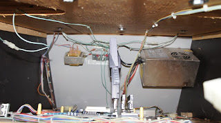

Q&A:

Which games work with the adapter?

Every game that can play on a 60 Hz SNES/SFC should work properly. This
includes games with co-processors (Super FX, DSP-1, SA1, etc), Super
Gameboy, Flash Carts, etc.


Which games DON'T work with the adapter?

The only known games that don't work are a small subset of PAL (European
 region) games, which are software locked to 50 Hz. These read the PPU
to determine whether they're running at 50 Hz or 60 Hz, and if they
detect 60 Hz, they show a message saying "THIS GAME PAK IS NOT DESIGNED
FOR YOUR SUPER FAMICOM OR SUPER NES". The NSS runs at 60 Hz, so without a
 hardware modification, these games will not work. There are VERY few
games that have this region lockout, and a flash cart like the SD2SNES
performs automatic region patching, which should take care of that
problem.


How about Super Scope 6, Mario Paint, or other games that use special controllers?

Okay... fine, they don't work either, simply because the Super System
motherboard doesn't have controller ports to plug the special
controllers into.


Do flash carts work?

The SNES PowerPak works out of the box. The SD2SNES requires a
modification to the motherboard for the reset circuit.  I don't have an
Everdrive, and I'm not sure that anyone has tested it... but it should
work, though possibly requiring the same reset modification as the
SD2SNES.


Do I need a new BIOS?

No, this works with any stock BIOS, though the V3 BIOS has some nice
features (like being able to reset to the main menu while in the middle
of a game).


What's the difference between the Basic and Deluxe models?

The Basic model will let you play most SNES games. The Deluxe model
includes the CIC lockout circuit, which increases compatibility to near
100%. The Deluxe model also includes a plastic support bracket, which
prevents you from inserting an SNES cartridge backwards. The Basic model
 will be perfectly fine for most games, especially if you're planning to
 simply install one game and leave it (like those that just want Super
Mario Kart or Legend of Zelda in their cabinet).


Which games require the CIC?

All SA1 games (Super Mario RPG, Kirby Super Star, Kirby's Dream Land 3,
and others) will require the CIC. I'm not aware of any, but there may
also be others that require either the CIC, or one or more of the CIC
signals as well. A list of SNES games and their enhancement chips can be
 found here: ... The SNES PowerPak does not require the CIC, though I'm not sure about the Everdrive or SD2SNES.


Can I slide the tray in and out with the cartridges in? With this adapter, you need to install the SNES cartridges with the tray in, and remove them before pulling the tray out. Honestly, swapping cartridges without pulling the tray is easier... the reach to get to the cartridge is the same as the reach to undo the latches that let the tray slide out, and the Timed/Skill switch is facing the front, so you can easily toggle back and forth. There is plenty of room for the cartridges inside the cabinet. If you really want to slide the tray in and out, some SNES cartridge PCBs are short enough that they will slide in and out if you remove them from their cartridge shell. Which Super System games support "skill" mode? ActRaiser, Addams Family, Lethal Weapon, Robocop 3, and Magic Floor (homebrew by nocash). What about Super System games with DIP switches? There is no hardware DIP switch support, but I have created an application (for Windows) which allows you to patch the ROMs with your desired DIP switch settings, here: http://retro-repairs.netai.net/nintendo_super_system/nss_dips.rar [264KB]. The same games which support "skill" mode also support DIP switches.Thanks to:
Martin Korth (nocash) for reverse engineering the Instruction ROM, removing the need for the security PROM... plus general SNES/NSS related information. Maximilian Rehkopf (ikari_01) for creating the SuperCIC CIC clone. MAME Team
+++++++++++++++++++++++++
Another question: Can you load more than 3 games at once?
Answer: No and yes, again.
When loading actual NSS-made games, you can only have 3 titles running off the board
at once. However, if I'm able to get a SNES to NSS adapter going... I can fit literally
hundreds upon hundreds of titles on 1 cartridge! How you might ask? By adding another
adapter to the adapter known as the 'SD2SNES.'


Description
The SD2SNES is a flashcart, which loads the ROMs in
the console itself. The handling of the flashcart is very simple. Just
put your back-up game ROM files on your SD card. Plug your SD card into
your SD2SNES and your SD2SNES into the cart slot of your system.Features
- SD/SDHC/SDXC support (tested up to 64GB; no exFAT support so SDXC cards must be reformatted using FAT32).
- High quality push to push memory card slot.
- Fast ROM loading (~9MB/s).
- Fast menu navigation.
- Directories are sorted automatically, no need for FAT sorting tools.
- High resolution menu (512×224) for adequate display of long file names.
- Real Time Clock.
- Supports ROM size up to 128Mbit (96Mbit actually implemented).
- Automatic near-time SRAM saving to SD Card (while the game is running). Some limitations apply:
- Near-time saving is switched to periodic saving when a game is found to use the SRAM as work RAM.
- Automatic saving is disabled when MSU1 is used. SRAM is saved on reset.
- Enhancement chip support (see below for implementation status).
- SuperCIC key (SNES CIC clone):
- Enables operation on unmodified consoles of all regions.
- Supports software 50/60Hz switching on SuperCIC enhanced consoles only (to be performed by SD2SNES firmware, not yet implemented there).
- Auto region patching: Eliminates “This Game Pack is not designed…” messages regardless of 50/60Hz setting.
ENHANCEMENT CHIPS:
Each supported enhancement chip can be used in conjunction with MSU1.
IMPLEMENTED:
BS-X memory map / Satellaview base unit registers (clock)
DSP1 / 1b
DSP2
DSP3
DSP4
ST-010
Cx4
MSU1
S-RTC
Cartridge uses custom made multi region shell. It fits in both American, Europe and Japan systems.
Downloads:
-Firmware Downloads-
http://retro-repairs.netai.net/sd2snes/sd2snes_firmware_v0.1.1_to_0.1.7b.rar
Instructions:
Download the zip file and extract to your SD card. Make sure the directory structure from the zip file is preserved, so you end up with a ‘sd2snes’ directory in the root of your SD card.Insert the card into your sd2snes and turn on the SNES. sd2snes will update its firmware from the card and boot.
After updating you may delete the ‘firmware.img’ file. You may not delete any other files from the sd2snes directory.
Important:
The ‘sd2snes’ directory is considered a system folder and ignored by the file browser. Do not put any ROMs there as they will not show up :)The headerless BS-X BIOS is required for running BS games. Rename it as ‘bsxbios.bin’ and put it in the sd2snes directory.
For DSPx / ST0010 support you need the DSP ROM dumps:
http://retro-repairs.netai.net/sd2snes/sd2snes_bios.rar
SD2SNES
Developed by: ikari_01Manufactured by: Krikzz
Worldwide sales by: DragonBox.de, emere.es, Stone Age Gamer, RetroGate
Additional sales by: Various
Also Known As: -
Review by Qtis – Completed 26/09/14
Introduction
The Super Nintendo Entertainment System, more commonly known as the SNES, was released around the world in the early 90's and ended up being the most successful console of its generation. It fought alongside the Sega Genesis/Megadrive, but managed to beat the other large console maker at the time. The SNES also brought forth new game series with games such as F-Zero, Pilotwings, Super Mario Kart and Super Mario RPG. The same games, which have been fan favorites and have seen new releases on even the latest generation of consoles. For the modern gamer, the problem of relatively small sales of niche games at the time have made quite a few games hard to find unless you're ready to pay an arm and a leg for a working copy. Emulation for the SNES is widely available, but has had its problems with supporting special chips and creating the genuine feeling of using original hardware.When the 21st century started rolling along, electronics started going down in price in terms of powerful chips and hardware. Old consoles began seeing development projects, such as the sd2iec for the Commodore 64, making the old devices work with modern storage options, mainly CF/SD cards. Add to this the interest for the SNES by many developers and modders for enabling region free mods by digging into the SNES CIC among other things (SNES CIC reverse engineering, 50/60Hz switching) as well as making more memory available for the games (Media Streaming Unit-1 or MSU1 (alternative mirror as byuu changes hosts)). At the same time the idea of creating a complete all in one solution for the SNES with most if not all special chips supported in one cart began forming in the heads of a few people around the SNES developers forums. As always with these kinds of projects for old hardware, open source was the way to go. Finally the last ingredient needed for making something special for the SNES was ikari_01, who began work on the prototype of a new solution for the SNES in 2009.
Thus, the Project SD2SNES was born.
Important GBAtemp Information:
GBAtemp has opened all reviews for user comment. Please remember that the comments must adhere to our strict guidelines. We ask that you do not post congratulatory comments or comments speculative in nature, negative in nature, or the like, that have nothing to do with the review or the review’s contents. Please consider posting only well researched comments that further the overall effect of the review and nothing more.
Special Thanks:
A special thanks must go out to ikari_01 for the support during the review as well as to Krikzz and Retrogate for providing the review sample. Retrogate is the officially licensed store for all Krikzz Flash Kit products and also handles sales of the SD2SNES. Their customer service, e-mail support, and inclusion of a tracking number make it easy to recommend them.
Product Information
The product information is from the SD2SNES project page retrieved during the reviewing of the cart. The software features may change as new versions of the operating system are released, but the hardware specifications are final.Features:
- SD/SDHC/SDXC support (tested up to 64GB; no exFAT support so SDXC cards must be reformatted using FAT32)
- High quality push-push memory card slot
- Fast ROM loading (~9MB/s)
- Fast menu navigation
- Directories are sorted automatically, no need for FAT sorting tools
- High resolution menu (512×224) for adequate display of long file names
- Real Time Clock
- Supports ROM size up to 128MBit (96Mbit actually implemented as there are no larger known memory maps)
- Automatic near-time SRAM saving to SD Card (while the game runs). Some limitations apply:
- Near-time saving is switched to periodic saving when a game is found to use the SRAM as work RAM.
- Automatic saving is disabled when MSU1 is used. SRAM is saved on reset.
- Enhancement chip support (see below for implementation status)
- SuperCIC key (SNES CIC clone):
- Enables operation on unmodified consoles of all regions
- Supports software 50/60Hz switching on SuperCIC enhanced consoles only (to be performed by sd2snes firmware, not yet implemented there)
- Auto region patching: eliminates “This Game Pak is not designed…” messages regardless of 50/60Hz setting
- Supports up to 16000 files per directory / roughly 50000 files per card
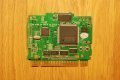
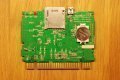
- BS-X memory map / Satellaview base unit registers (clock)
- DSP1 / 1b
- DSP2
- DSP3
- DSP4
- ST-010
- Cx4
- MSU1
- S-RTC
- OBC1
The SD2SNES is not produced by ikari_01 anymore, but do not worry. Krikzz, known for the Everdrive series of Flash Kits, has taken over the production and distribution of the cart. This means that the cart is available in almost all stores selling the Everdrives and the build quality will be similar to Everdrive series.
Contents, Packaging, Design & Impressions
Contents:- 1x SD2SNES Flash Kit inside a universal SNES shell
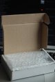
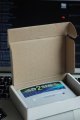
The SD2SNES supplied by RetroGate follows the same packaging system as used by other carts produced by Krikzz. The shipment was shipped inside a bubble wrap envelope and the cart itself was inside a white cardboard box with a label Everdrive - Krikzz.com on top. The SD2SNES itself was loose inside the box with extra supporting bubble wrap . The good packaging made sure that the review unit arrived in one piece without any damage to the case.
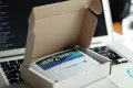
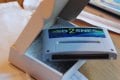
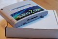
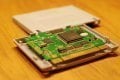
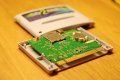
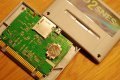
Setup & Usage
The SD2SNES, as its name suggests, requires a SD card to function. The SD2SNES also supports microSD/miniSD cards via SD card adapters. At the time of writing, SD, SDHC and SDXC cards are supported up to 64GB, though larger cards need to be formatted with FAT32 as exFAT isn't supported (yet). The operating system is available for download from the developer's home page and the downloaded zip file includes an image for preparing the SD card for the cart: drag and drop the sd2snes folder to the root of the SD card and you're done. At the time of writing the latest OS version is v0.1.6, though v0.1.7 is right around the corner with additional features including cheat support.The device loads the OS and games from a single SD card placed in the spring-loaded SD card slot on the top of the cart. Since the sd2snes folder is hidden by the SD2SNES firmware on boot, all homebrew and games will need to be placed somewhere else on the SD card. In case you want to remove the need to cycle through a load of folders, you can just dump all your games on the root of your SD card. The SD2SNES supports up to 16000 files per directory, but I'd personally recommend using some kind of folder system instead of placing the whole romset on the root of the SD card. Once you boot your SNES with the SD2SNES inserted, you will be presented with a list of your SD card's root without the sd2snes folder.
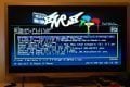
Saving with the SD2SNES is as simple as it gets. In most games, the save is transferred to the SD card immediately as you save. As the SRAM is battery-based, you can be guaranteed that the save is kept on the cart even in the extreme case that a power outage interrupts your gaming. In case the game uses the SRAM as work RAM (as in needs the extra RAM to run), the saving will be changed to periodic saving. Here the save is routinely transferred to the SD, but may not be immediate as the SRAM is used for more than just saving. Unfortunately save states are impossible to make with the SNES in general, since the APU state cannot be snapshot after it has code running (mentioned by ikari_01 here).
MSU1 is a tricky thing in terms of real time saving, since the custom chip system doesn't support flow control. This has been explained by ikari_01 in the comment section of SD2SNES.de, but isn't a problem as long as you remember to reset the console. Since MSU1 is a relatively new thing, not many hacks or games use it to the fullest and/or are completely finished. As the SNES scene and especially the SD2SNES have shown, this will probably not be the situation in the future. MSU1's 4GB of space for a SNES game with CD quality audio can be considered a revolution for the SNES. Byuu has shown SNES games such as Chrono Trigger with the PlayStation version's FMVs included via MSU1 support. It's amazing to see such options made available on original hardware and without any modifications to the console itself. And who said old consoles couldn't innovate?
Compatibility
Compatibility of a cart like the SD2SNES is the number one thing on many a buyer's checklist. This is why I paid extra attention to special chip support and how games reacted to the cart if a special chip was used. The testing hardware was a PAL SNES with 50/60Hz and Region Free modifications, though both mods were set to standard 50 Hz and PAL region for testing purposes. All testing was done with clean ROMs from the GoodSNES set without any region patches or hacks unless otherwise specified (such as translations or the SDD-1 patch for Star Ocean). If a game uses a special chip, the chip is mentioned after the verdict.
Unsupported Games list:
Carts with BS memory pack slots, other than BS-X BIOS (e.g. Derby Stallion 96, any Tsukuuru). They may run but cannot use memory pack related features.
Sufami Turbo games:
Carts with BS memory pack slots, other than BS-X BIOS (e.g. Derby Stallion 96, any Tsukuuru). They may run but cannot use memory pack related features.
Sufami Turbo games:
- Car Ranger
- Crayon Shin Chan
- Gegege No Kitarou
- Gekisou Sentai Carranger: Zenkai Racer Senshi
- Poi Poi Ninja
- Sailor Moon Stars Panic 2
- SD Gundam Generations: part 1
- SD Gundam Generations: part 2
- SD Gundam Generations: part 3
- SD Gundam Generations: part 4
- SD Gundam Generations: part 5
- SD Gundam Generations: part 6
- SD Ultra Battle: Seven Legend
- SD Ultra Battle: Ultraman Legend
- Sufami Turbo hardware
- Tetris 2+ Bombliss
- Dirt Racer
- Dirt Trax FX
- Doom
- Star Fox 2
- Star Fox / Starwing
- Stunt Race FX / Wild Trax
- Super Mario World 2: Yoshi’s Island
- Vortex
- Winter Gold / FX Skiing
- Daisenryaku Expert WWII: War in Europe
- Derby Jockey 2
- Dragon Ball Z: Hyper Dimension
- Habu Meijin no Omoshiro Shogi
- Itoi Shigesato no Bass Tsuri No. 1
- Jikkyou Oshaberi Parodius
- J.League ’96 Dream Stadium
- Jumpin’ Derby
- Kakinoki Shogi
- Kirby’s Dream Land 3
- Kirby Super Star
- Marvelous: Mouhitotsu no Takarajima
- Masters New: Haruka Naru Augusta 3
- Mini 4WD Shining Scorpion Let’s & Go!!
- Pebble Beach no Hotou: New Tournament Edition
- PGA European Tour
- PGA Tour ’96
- Power Rangers Zeo: Battle Racers
- SD F-1 Grand Prix
- SD Gundam G NEXT
- Shin Shogi Club
- Shogi Saikyou
- Shogi Saikyou 2
- Super Bomberman Panic Bomber World
- Super Mario RPG: Legend of the Seven Stars
- Super Robot Taisen Gaiden: Maso Kishin – The Lord Of Elemental
- Star Ocean (unhacked version)
- Street Fighter Alpha 2 / Zero 2
- Hayazashi Nidan Morita Shougi
- Hayazashi Nidan Morita Shougi 2
- Far East of Eden Zero
- Momotaro Dentetsu Happy
- Super Power League 4
Testing the
SD2SNES was done with a 16GB SanDisk Ultra Class 10 UHS-1 card. In order
to remove any problems with the file system or corruption, the card was
formatted to FAT32 with the Windows Formatter. All cards should work
with the device and offer the same compatibility, but MSU1 compatibility
requires an access time of around up to 1 ms. The access time
requirement is needed due to the simultanious streaming of audio and
data on MSU1 games. Fast transfer speeds do not automatically mean fast
access times, so keep this in mind if you plan to take advantage of MSU1
support.
 The results are color-coded. Green is for a game which works without
issues, yellow is for a game with issues and red is for a game which
won't run. For the games which failed, multiple versions were tested to
ensure that it wasn't a case of a bad ROM or unsupported version.
The results are color-coded. Green is for a game which works without
issues, yellow is for a game with issues and red is for a game which
won't run. For the games which failed, multiple versions were tested to
ensure that it wasn't a case of a bad ROM or unsupported version.
Super Nintendo Entertainment System:
Note: Satellaview games are unique games for the Satellaview modem add-on.
The SD2SNES was not designed to be the cheapest option available and it shows. Paying a bit extra adds functions not available to cheaper options. Speical chip support for games like Mario Kart (DSP) and Megaman X2 (Cx4) are clear indicators that the SD2SNES can do much more than just play normal SNES games. The hardware can be seen as the ultimate solution for the SNES with little trade-offs. Still, there are a few caveats including the lack of GSU1/2 (SuperFX) and SA-1 support. These games are only a few percent of the total library of games for the SNES, but include some of the most iconic games ever released for the SNES. I would still not be let down by the current situation, since development has brought support for new chips even this year (2014)!
And as some people will prefer this:
TL;DR: The SD2SNES has been and still is at the time of writing the best Flash Kit available for the SNES. If you want the best out of the best and are willing to pay a little extra for the additional features and support, you won't be disappointed.
Super Nintendo Entertainment System:
- Actraiser [PAL] - PASS
- Aladdin [PAL] - PASS
- Another World [PAL] - PASS
- Bahamut Lagoon [NTSC/J] (w/ DeJap English Translation) - PASS
- Breath of Fire [NTSC/U] - PASS
- Castlevania - Vampire's Kiss [PAL] - PASS
- Chrono Trigger [NTSC/U] - PASS
- Clock Tower [NTSC/J] (w/ Aeon Genesis English Translation) - PASS
- Dai Kaiju Monogatari 2 [NTSC/J] - PASS [S-RTC]
- Donkey Kong Country - PASS
- Dragon Ball Z Super Saiya Densetsu [NTSC/J] (w/ Klepto Software English Translation) - PASS
- Dragon Quest V Tenkuu no Hanayome [NTSC/J] (w/ DeJap English Translation) - PASS
- Dungeon Master [NTSC/U] - PASS [DSP-2]
- Earthworm Jim [PAL] - PASS
- Earthbound [NTSC/U] - PASS
- F1 ROC II: Race of Champions [NTSC/U] - PASS [ST-010]
- F-Zero [PAL] - PASS
- Famicom Tantei Club Part II (w/ Neo Demiforce English Translation) - PASS
- Final Fantasy III [NTSC/U] - PASS
- Final Fantasy V [NTSC/J] (w/RPGe patch) - PASS
- The Flintsones [PAL] - PASS
- Gradius III [NTSC/U] - PASS
- Harvest Moon [PAL] - PASS
- Illusion of Time [PAL] - PASS
- Joe and Mac 3 - Lost in the Tropics [PAL] - PASS
- JoJo no Kimyou na Bouken [NTSC/J] (w/ Aeon Genesis English Translation) - PASS
- Killer Instinct [PAL] - PASS
- Kirby's Ghost Trap [PAL] - PASS
- Legend of Zelda, The - A Link to the Past [PAL] - PASS
- Live-a-Live [NTSC/J] - PASS
- Megaman 7 [PAL] - PASS
- Megaman X [PAL] - PASS
- Megaman X2 [PAL] - PASS [Cx4]
- Megaman X3 [PAL] - PASS [Cx4]
- Metal Combat: Falcon's Revenge [PAL] - PASS [OBC-1]
- Might & Magic 3: Isles of Terra [U] - PASS
- Mortal Kombat 3 [PAL] - PASS
- Ninja Gaiden Trilogy [NTSC/U] - PASS
- Ninjawarriors - The New Generation [PAL] - PASS
- Ogre Battle - The March of The Dark Queen [NTSC/U] - PASS
- Phalanx [PAL] - PASS
- Pilotwings [NTSC/U] - PASS [DSP-1]
- Rockman & Forte [NTSC/J] - PASS
- Romancing Sa-Ga 3 [NTSC/J] (w/ Mana Sword English Translation) - PASS
- SD Gundam GX [NTSC/J] - PASS [DSP-3]
- Secret of Evermore [PAL] - PASS
- Secret of Mana [PAL] - PASS
- Seiken Densutsu 3 [NTSC/J] - PASS
- Shin Megami Tensei [NTSC/U] (w/ Aeon Genesis English Translation) - PASS
- Star Ocean [NTSC/J] SDD-1 Hack - PASS [SDD-1]
- Super Ghouls 'n Ghosts [PAL] - PASS
- Super Mario All-Stars + Super Mario World [PAL] - PASS
- Super Mario Kart [PAL] - PASS [DSP-1/1B]
- Super Metroid [PAL] - PASS
- Super Street Fighter II [PAL] - PASS
- Tales of Phantasia [NTSC/J] (w/ DeJap English Translation) - PASS
- Terranigma [PAL] - PASS
- Top Gear 3000 [PAL] - PASS [DSP-4]
- Treasure Hunter G [NTSC/J] (w/ Metalhawk English Translation) - PASS
- Ultima - The False Prophet [NTSC/U] - PASS
- Wonder Project J - Kikai no Shounen Pino [NTSC/J] (w/ WakdHacks English Translation) - PASS
- Zombies (PAL) - PASS
Note: Satellaview games are unique games for the Satellaview modem add-on.
- As mentioned before, Bokujou Monogatari - Dai-2-wa - PASS
- BS Fire Emblem - Akaneia Senki Hen - Dai-1-wa - Palace Kanraku - PASS
- BS F-Zero Grand Prix - Dai-1-shuu - Knight League - ISSUES (Game freezes after entering game specific area)
- BS Super Mario USA - Power Challenge - Dai-1-kai - PASS
- Chrono Trigger - Jet Bike Special - PASS
- Chrono Trigger - Music Library - PASS
- Excitebike - Bunbun Mario Battle - Stadium 1 - PASS (Demo intro runs for a few minutes before you can play.)
- Kirby no Omochabako - Hoshi Kuzushi - ISSUES (Problems with proceeding while loading game parts)
- Mario Paint - BS Ban - PASS
- Panel de Pon - Event '98 - PASS
- Yoshi no Panepon - BS Ban - PASS
- Astrohawk - FAIL (Black screen on boot)
- Airwolf - PASS (Garbled graphics also happen on emulator)
- Bio Worm - PASS
- BLT - ISSUES (Garbled graphics in the lower left area on the screen)
- Classic Kong - PASS
- Hong Kong 97 - PASS
- N-Warp Daisakusen (v 1.1) - PASS
- Skipp and Friends - PASS
- Super Mario Odyssey - PASS [MSU1]
- Uwol - Quest for Money - PASS
Conclusions
Many people have asked again and again why someone would spend money on a Flash Kit for a console released almost 25 years ago and which has highly compatible emulators such as bsnes available. The fight between original hardware and emulation will never end, but devices such as the SD2SNES make it hard to not recommend the original over the new wave. Just looking at the features and the nice row of green PASS verdicts should be enough for anyone sceptical of the execution of the SD2SNES. As new features and support for more special chips are developed by ikari_01 and the community, you can expect more use out of your device.The SD2SNES was not designed to be the cheapest option available and it shows. Paying a bit extra adds functions not available to cheaper options. Speical chip support for games like Mario Kart (DSP) and Megaman X2 (Cx4) are clear indicators that the SD2SNES can do much more than just play normal SNES games. The hardware can be seen as the ultimate solution for the SNES with little trade-offs. Still, there are a few caveats including the lack of GSU1/2 (SuperFX) and SA-1 support. These games are only a few percent of the total library of games for the SNES, but include some of the most iconic games ever released for the SNES. I would still not be let down by the current situation, since development has brought support for new chips even this year (2014)!
And as some people will prefer this:
TL;DR: The SD2SNES has been and still is at the time of writing the best Flash Kit available for the SNES. If you want the best out of the best and are willing to pay a little extra for the additional features and support, you won't be disappointed.
Verdict
| Pros + Easy to use (drag and drop to SD card) + Hardware build quality and universal shell design + Special chip support beats all other options available + Fantastic compatibility for ROMs, Homebrew, Satellaview and MSU1 + Support from developer is very good + New features added with new OS releases + Open source and well documented operating system + SRAM backup of saves are instant + SuperCIC and In-game reset compatibility with a hardware mod + File limit per directory (16000 per folder) |
Cons - GSU1/2 (SuperFX), SA-1 and a few other special chips are yet to be supported. - Cheat support (to be released in v0.1.7) |
| 9.7
out of 10
|
Overall
Easily the best Flash Kit available for the SNES. If you're interested in the best overall compatibility as well as on-going support to add even more features, you can't go wrong. The device itself is easy to use and offers fantastic features to both untouched as well as modded consoles. A few unsupported special chips drop the score a few points, but as the software and hardware are as stellar as they are, I can't justify a lower score. Krikzz's hardware quality as well as ikari_01's and the community's software updates will guarantee you many hours of fun on your SNES with even more functions than ever seen before. |
+++++++++++++++++++++++++
I also found this forum topic on the NSS here.. http://forums.nesdev.com/viewtopic.php?f=12&t=9065
I also found this forum topic on the NSS here.. http://forums.nesdev.com/viewtopic.php?f=12&t=9065
nocash
|
||||
Joined: Fri Feb 24, 2012 12:09 pm Posts: 487 |
|
|||
| Top | ||||
| byuu |
|
|||
Joined: Mon Mar 27, 2006 5:23 pm Posts: 1147 |
|
|||
| Top | ||||
| nocash |
|
|||
Joined: Fri Feb 24, 2012 12:09 pm Posts: 487 |
|
|||
| Top | ||||
| byuu |
|
|||
Joined: Mon Mar 27, 2006 5:23 pm Posts: 1147 |
|
|||
| Top | ||||
| tepples |
|
|||
Joined: Sun Sep 19, 2004 11:12 pm Posts: 16838 Location: NE Indiana, USA (NTSC) |
|
|||
| Top | ||||
| nocash |
|
|||
Joined: Fri Feb 24, 2012 12:09 pm Posts: 487 |
|
|||
| Top | ||||
| byuu |
|
|||
Joined: Mon Mar 27, 2006 5:23 pm Posts: 1147 |
|
|||
| Top | ||||
| tepples |
|
|||
Joined: Sun Sep 19, 2004 11:12 pm Posts: 16838 Location: NE Indiana, USA (NTSC) |
|
|||
| Top | ||||
| byuu |
|
|||
Joined: Mon Mar 27, 2006 5:23 pm Posts: 1147 |
|
|||
| Top | ||||
| nocash |
|
|||
Joined: Fri Feb 24, 2012 12:09 pm Posts: 487 |
|
|||
| Top | ||||
| nocash |
|
|||
Joined: Fri Feb 24, 2012 12:09 pm Posts: 487 |
|
|||
| Top | ||||
| nocash |
|
|||
Joined: Fri Feb 24, 2012 12:09 pm Posts: 487 |
|
|||
| Top | ||||
| Memblers |
|
|||||
Joined: Mon Sep 20, 2004 6:04 am Posts: 3273 Location: Indianapolis |
|
|||||
| Top | ||||||

| byuu |
|
|||
Joined: Mon Mar 27, 2006 5:23 pm Posts: 1147 |
|
|||
| Top | ||||
| nocash |
|
|||||||||||||||||||||||||||||||||||||||||||||||||||||||||||||||||||||||||||||||||||||||||||||||||||||||||||||||||||||||||||||||||||||||||||||||||||||||||||||||||||||||||||||||||||||||||||||||||||||||||||||||||||||||||||||||||||||||||||||||||||||||||||||||||||||||||||||||||||||||||||||||||||||||||||||||||||||||||||||||||||||||||||||||||||||||||||||||||||||||||
Joined: Fri Feb 24, 2012 12:09 pm Posts: 487 |
| |||||||||||||||||||||||||||||||||||||||||||||||||||||||||||||||||||||||||||||||||||||||||||||||||||||||||||||||||||||||||||||||||||||||||||||||||||||||||||||||||||||||||||||||||||||||||||||||||||||||||||||||||||||||||||||||||||||||||||||||||||||||||||||||||||||||||||||||||||||||||||||||||||||||||||||||||||||||||||||||||||||||||||||||||||||||||||||||||||||||||

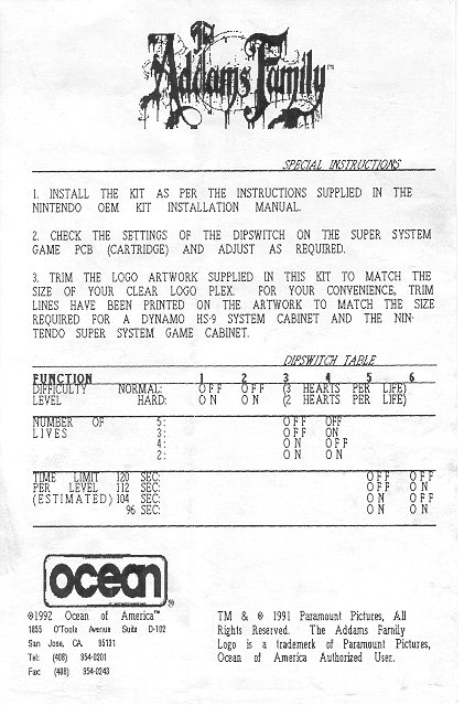
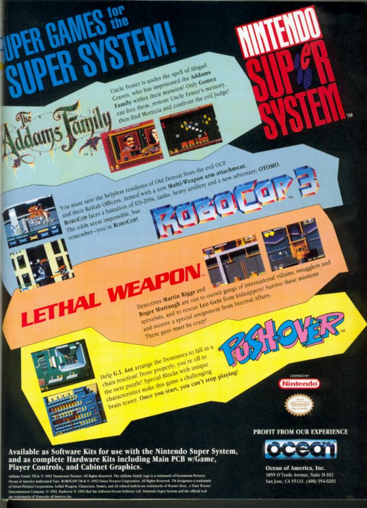
Thank you because you have been willing to share information with us. we will always appreciate all you have done here because I know you are very concerned with our. Arcade toronto
ReplyDeleteWho ever knew that an Italian plumber could go so far? Certainly Super Mario has opened our eyes for decades, ever since it became public, super Mario has captured the attention of a young generation of video game players who used Nintendo's equipment. The very first stand alone consoles that were compatible with the oldest versions of Super Mario were big and looked like a small stove, but the game was excellent none the less! twitch viral
ReplyDelete